
Method and apparatus for controlling crosstalk, power and yield in nanometer technology ICs

a technology of crosstalk and nanometers, applied in the field of nanometer technology ics, can solve the problems of inducing glitches and timing errors, crosstalk making a-priori prediction of timing closure difficult or impossible, and no optimal trade-off between resizing cells, etc., to reduce or eliminate crosstalk violations, minimize power, and minimize coupling capacitance

Inactive Publication Date: 2009-02-17
WEISS JONATHAN
View PDF5 Cites 5 Cited by
  • Summary
  • Abstract
  • Description
  • Claims
  • Application Information

AI Technical Summary

Benefits of technology

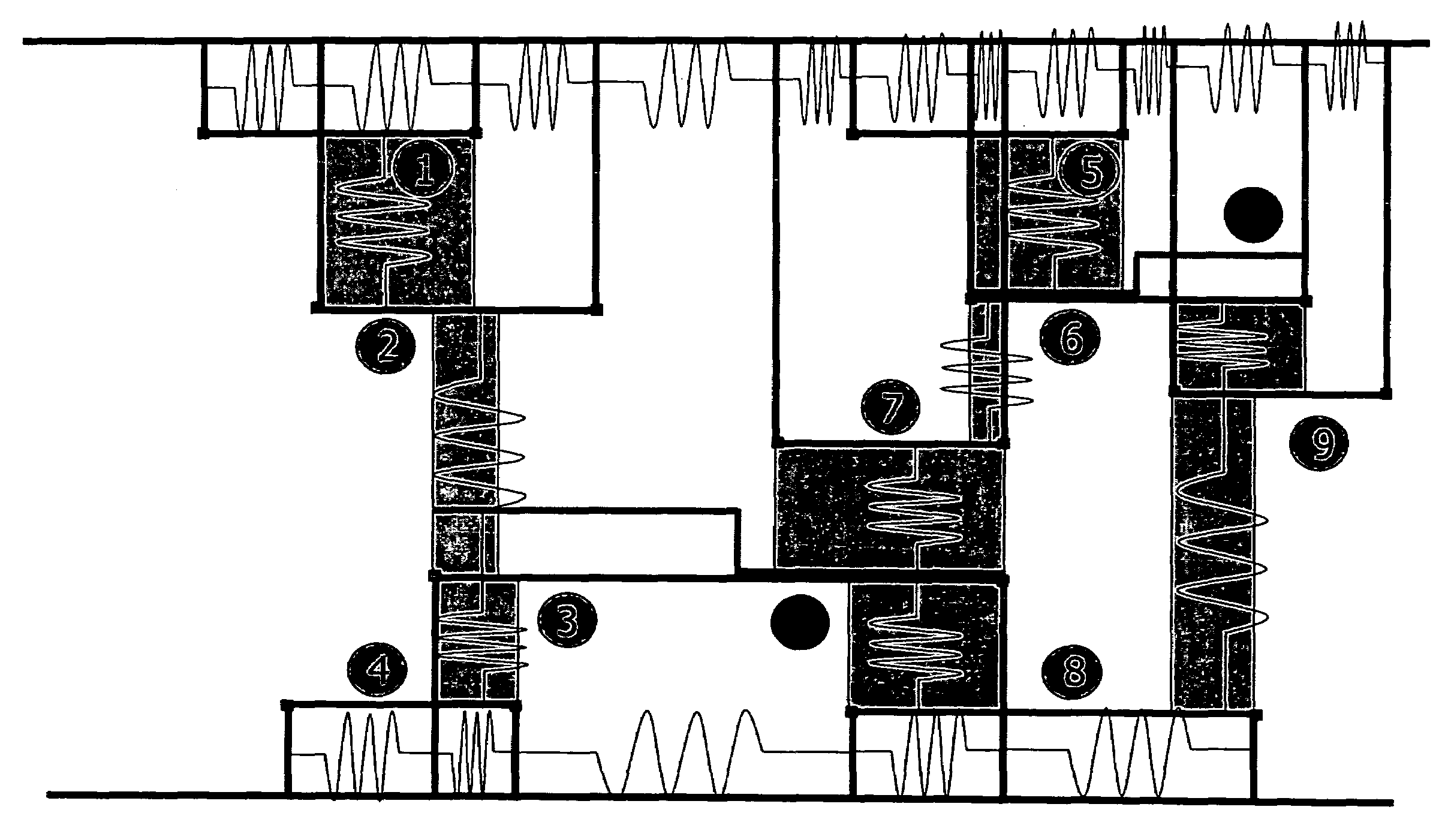
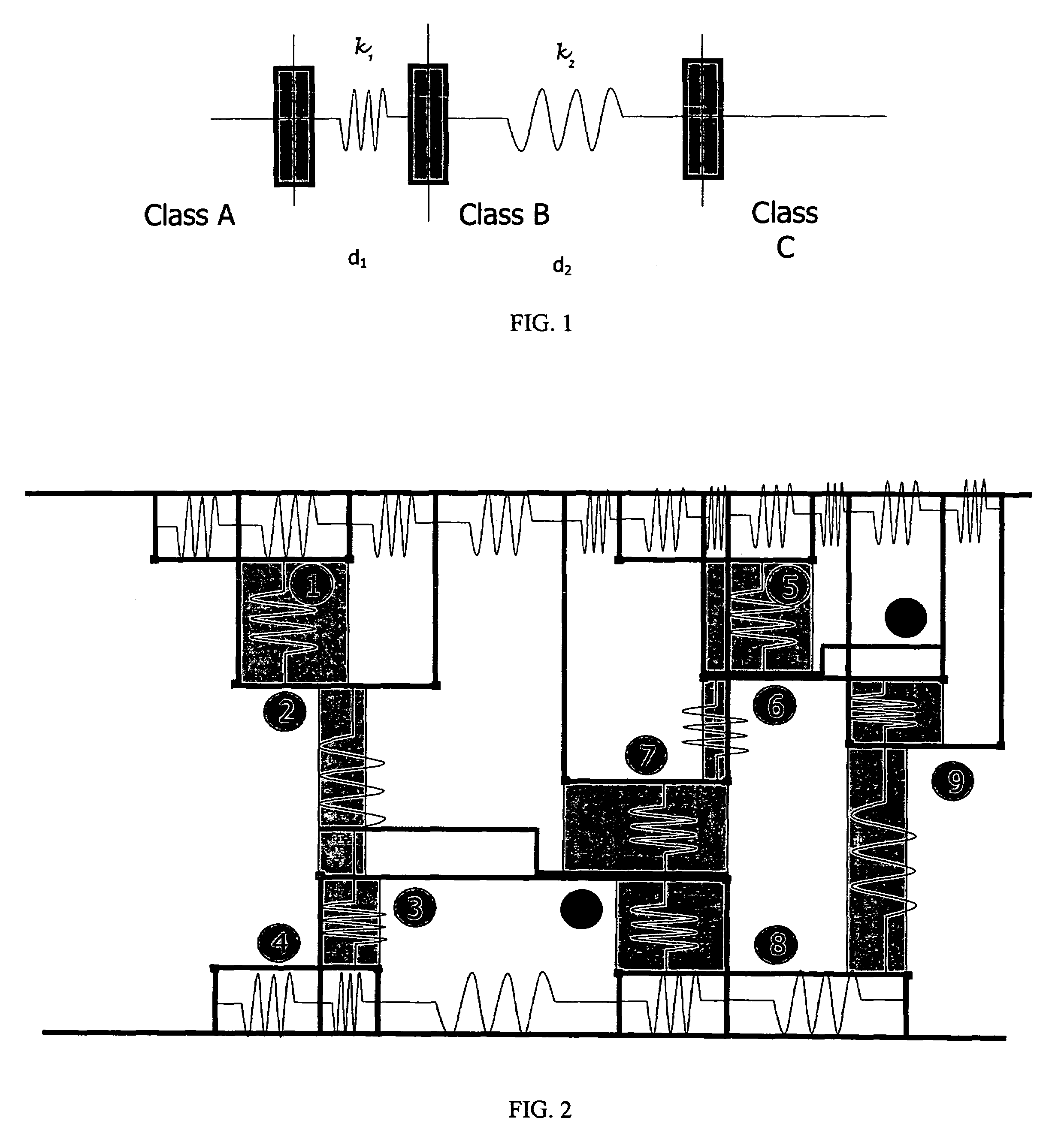
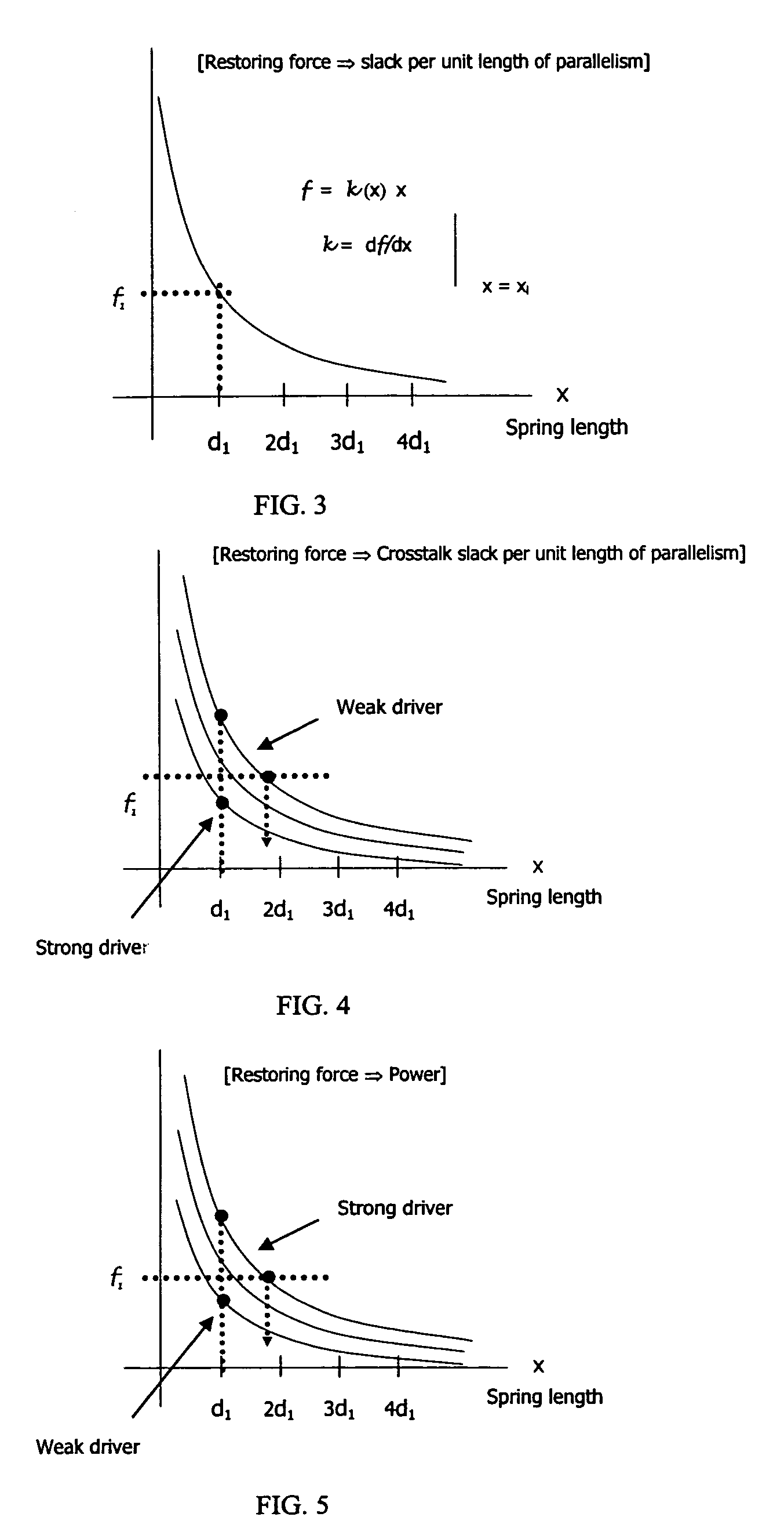
[0011]A method for controlling crosstalk, power and yield in nanometer-technology integrated circuits (“ICs”) is based on a performance driven space optimization technique that minimizes the coupling capacitance between the interconnecting wires. Given a routed IC design, virtual compression-springs are inserted between all the elements of the design creating a mesh of springs. The design is then perturbed, or shaken, by transforming the spring system into a minimum-energy problem, a solution for which reduces or eliminates crosstalk violations, minimizes power and increases yield as the springs reach minimum energy state. One described embodiment of the method comprises a two-step automatic process that needs no user input once a physical layout of the IC has been provided to the apparatus. In the described method, the primitives of a given IC layout are defined in terms of object points. Each primitive is a separate geometric region. All the primitives of a given layout have inter-related electrical properties that are very complex and that depend on many different variables. In a first step of the described method, a mesh of virtual compression springs connecting all the layout primitives is generated from the object points. The spring constant for each virtual spring embedded between interconnecting wires is chosen to follow a relationship between a slack function (crosstalk and power) and the separation distance between the interconnecting wires. For crosstalk for example, a suitable relationship can be derived by performing transmission line analysis and simulation. Other spring constants may be derived from the physical properties of the layout. In a second step of the described method, the design is shaken by minimizing the energy of the virtual compression-spring-loaded-system, resulting in new object points and new positions for the springs and the interconnecting wires. As the interconnecting wires move apart, their coupling capacitances is reduced, and consequently crosstalk and power are minimized, yield is maximized as long as sufficient space is available within the chip area.

Problems solved by technology

In nanometer process geometries, issues relating to timing, signal integrity, manufacturing and time to market are presenting new challenges to designers and EDA tools.
Crosstalk, which is the most common and severe signal integrity problem, may cause induced glitches and timing errors.
Crosstalk makes a-priori prediction of timing closure difficult or impossible.
However, there is no way to optimally trade-off between resizing cells and fine-tuning the coupling capacitances, forcing designers to use either method, or both, in brute force.
Power consumption has been growing exponentially with each process generation.
Fixing crosstalk by upsizing cells and inserting delay cells makes a bad situation worse with respect to power.
As coupling capacitances continue to increase, so does the switching noise—which is a direct result of the ever-shrinking process geometries.
Nevertheless, the ability to apply RET effectively is limited by the layout itself.
To follow best practices for example, designs are required to meet minimum design rules—spacing rules, reliability rules (via stacking and minimum area rules), and process antennas rules, making RET difficult to apply.
Because compaction is a 2-D NP-complete problem it is extremely difficult to solve.
Unfortunately, minimizing crosstalk between horizontal segments may maximize crosstalk between vertical segments, resulting in a redistribution of the problem.
Therefore, there is no trivial way to automatically control spacing and parallelism, which are both critical to minimizing the coupling capacitances.
During global routing, crosstalk estimation may be inaccurate, but the freedom to control crosstalk is nearly unrestricted.
On the other hand, during detail routing, crosstalk estimation may be more accurate, but the freedom to control crosstalk is more restricted.
When routing is over-constrained, irresolvable congestion problems often occur making it difficult to achieve 100% routing completion.
As a result, worse case rules are typically applied and difficulties with routing completion often occur.
Both of these rule classes suffer from severe limitations.
First, even though spacing is a two-dimensional problem, it is usually carried out as two independent, one-dimensional steps.
Second, current spacing algorithms adjust positions of the interconnecting wires locally within routing region, not globally within the entire routing area of an IC.
Third, it has been noted that the non-linearity of the objective functions involving crosstalk makes it difficult to develop efficient algorithms for their optimization.
However, depending on when rip-up and reroute is performed during the routing process, routing space may or may not be available, and rip-up may be so extensive that a complete re-route becomes necessary.
Although in general, post-routing optimization is less flexible in moving the interconnecting wires around than during detail routing, it is still the best way to reduce coupling capacitances and hence crosstalk between the interconnecting wires for a general layout problem.
All the primitives of a given layout have inter-related electrical properties that are very complex and that depend on many different variables.

Method used


Image

  • Method and apparatus for controlling crosstalk, power and yield in nanometer technology ICs
  • Method and apparatus for controlling crosstalk, power and yield in nanometer technology ICs
  • Method and apparatus for controlling crosstalk, power and yield in nanometer technology ICs

Examples


Embodiment Construction

[0018]The described method comprises a two-step automatic process that requires no user input once a geometric representation of the object has been provided to the apparatus. The primitives of a given IC layout are defined in terms of object points. Each primitive is a separate geometric region. All the primitives of a given layout have inter-related electrical properties, which are very complex and generally depend on many different variables. In a first step of the described method, a mesh of virtual non-linear compression springs connecting all the layout primitives is generated from the object points. Along each spring spacing, slack or power variations may be described.

[0019]The spring constant for each virtual spring embedded between interconnecting wires is chosen as follows:[0020]1. Unity spring constants for spacing variations.[0021]2. Non-linear spring constants for slack-variation versus separation distance derived from crosstalk specifications using signal integrity ana...


PUM


Abstract

A method for controlling crosstalk, power and yield in nanometer-technology integrated circuits (“ICs”) is based on a performance driven space optimization technique that minimizes the coupling capacitance between the interconnecting wires. Given a routed IC design, virtual compression-springs are inserted between all the elements of the design creating a mesh of springs. The design is then perturbed, or shaken, by transforming the spring system into a minimum-energy problem, a solution for which reduces or eliminates crosstalk violations, minimizes power and increases yield as the springs reach minimum energy state. In a described method, the primitives of a given IC layout are defined in terms of object points. In a first step, a mesh of virtual compression springs connecting all the layout primitives is generated from the object points. The spring constant for each virtual spring embedded between interconnecting wires is chosen to follow a relationship between a slack function and the separation distance between the interconnecting wires. In a second step, the design is shaken by minimizing the energy of the virtual compression-spring-loaded-system, resulting in new object points and new positions for the springs and the interconnecting wires.

Description

CROSS-REFERENCE TO RELATED APPLICATION[0001]This application claims the benefit of Provisional Patent Application No. 60 / 578,585, filed Jun. 10, 2004.TECHNICAL FIELD OF THE INVENTION[0002]The present invention relates generally to a method and apparatus for controlling crosstalk, power and yield in nanometer-technology ICs, and more particularly, to a method and apparatus that uses virtual compression springs to increase the separation distance between the interconnecting wires, reducing their coupling capacitance, and consequently minimizing or eliminating crosstalk, minimizing power and increasing yield when sufficient space is available within the chip area.BACKGROUND OF THE INVENTION[0003]In nanometer process geometries, issues relating to timing, signal integrity, manufacturing and time to market are presenting new challenges to designers and EDA tools. Timing is interconnects dominated. In 130 nm designs, for example, interconnect delay accounts for about 80% of the path delay...

Claims


Application Information

Patent Timeline
IPC IPC(8): G06F17/50
CPCG06F17/5036G06F17/5045G06F2217/08G06F30/30G06F30/367G06F2111/06
Inventor WEISS, JONATHAN
Owner WEISS JONATHAN
Learn More