Flash memory device and method of reading data from flash memory device

a flash memory and data technology, applied in the field of flash memory devices, can solve the problems of changing the programming state, increasing the noise of unselected bit lines, etc., and achieve the effect of reducing or eliminating coupling noise and minimizing coupling capacitan

Inactive Publication Date: 2009-06-23
SAMSUNG ELECTRONICS CO LTD
View PDF7 Cites 7 Cited by
  • Summary
  • Abstract
  • Description
  • Claims
  • Application Information

AI Technical Summary

Benefits of technology

[0017]Embodiments of the invention provide a flash memory device and related method of reading data from the flash memory device. The flash memory device is capable of pre-charging bit lines in a standby state to minimize coupling capacitance between adjacent bit lines during the read operation in order to reduce or eliminate coupling noise.

Problems solved by technology

This voltage increase on the unselected bit line acts as noise, potentially changing the programming state of a memory cell adjacent to the selected cell.

Method used


Image

  • Flash memory device and method of reading data from flash memory device
  • Flash memory device and method of reading data from flash memory device
  • Flash memory device and method of reading data from flash memory device

Examples


Embodiment Construction

[0029]Embodiments of the invention will now be described in some additional detail with reference to the accompanying drawings. The invention may, however, be embodied in many different forms and should not be construed as being limited to only the embodiments set forth herein. Rather, these embodiments are presented as teaching examples. Throughout the written specification and drawings, like reference numerals are used to refer to like or similar elements.

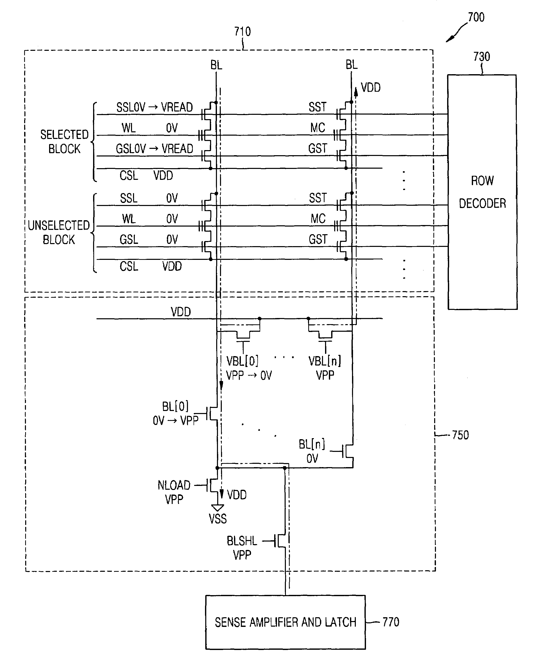
[0030]A flash memory device 700 according to an embodiment of the present invention will first be explained with reference to FIG. 7. FIG. 7 is intended to illustrate exemplary voltage conditions for the constituent signal lines of flash memory device 700 in a standby state according to an embodiment of the invention.

[0031]Flash memory device 700 generally includes a memory cell array 710, a row decoder 730, a column select circuit 750 and a sense amplifier 770. Memory cell array 710 of the flash memory device 700 includes at lea...


PUM


Abstract

A method of reading data from a flash memory device that includes a multiple block memory cell array, each block having a cell string connected to a bit line and comprising a string select transistor connected to a string select line, a memory cell connected to a wordline and a global select transistor connected to a global select line and having a source connected to a common source line. The method includes pre-charging the bit lines to a first voltage in a standby state, discharging a selected bit line connected to a selected memory cell to a second voltage in response to a read command, and reading data stored in the selected memory cell in response to the read command.

Description

BACKGROUND OF THE INVENTION[0001]1. Field of the Invention[0002]The present invention relates to a flash memory device. More particularly, the invention relates to a method of reading data from a flash memory device, which is capable of pre-charging bit lines in a standby state to minimize coupling capacitance between neighboring bit lines during the read operation in order to remove coupling noise.[0003]This application claims the benefit of Korean Patent Application No. 10-2006-0108529, filed on Nov. 3, 2006, the subject matter of which is hereby incorporated by reference.[0004]2. Description of the Related Art[0005]Semiconductor memory devices may be classified as volatile memory devices and non-volatile memory devices according to their ability to retain stored data in the absence of continuously applied power. The class of non-volatile memory devices includes electrically erasable and programmable read only memory (EEPROM).[0006]EEPROM operates in several fundamental modes, inc...

Claims


Application Information

Patent Timeline
Patent Type & Authority Patents(United States)
IPC IPC(8): G11C16/06
CPCG11C16/26G11C7/02G11C16/0483G11C16/08G11C16/24G11C16/30
Inventor KIM, HO-JUNG
Owner SAMSUNG ELECTRONICS CO LTD
Why Eureka
Try Eureka