Method for managing UV irradiation for curing semiconductor substrate

a technology of uv irradiation and curing substrate, which is applied in the direction of semiconductor/solid-state device testing/measurement, instruments, measurement devices, etc., can solve the problem of tending to drop in transmissivity, and achieve the effect of automatic control

Active Publication Date: 2009-03-10
ASM JAPAN
View PDF5 Cites 384 Cited by
  • Summary
  • Abstract
  • Description
  • Claims
  • Application Information

AI Technical Summary

Benefits of technology

[0012]In an embodiment of the present invention, a mechanism is provided whereby the lamp-based light source receives a feedback of illuminance information and increases the output to compensate for any drop in illuminance in order to maintain the illuminance at a constant level.
[0015]In an embodiment of the present invention, it is also possible to automatically control the cleaning time and frequency by using specific illuminance values as triggers.

Problems solved by technology

Depending on the material of the transmission window, however, its transmissivity tends to drop when the transmitting light is UV light, which carries high energy, due to deposits accumulating on the window material.

Method used


Image

  • Method for managing UV irradiation for curing semiconductor substrate
  • Method for managing UV irradiation for curing semiconductor substrate
  • Method for managing UV irradiation for curing semiconductor substrate

Examples


Embodiment Construction

[0026]The present invention will be explained in detail with reference to preferred embodiments. However, the preferred embodiments are not intended to limit the present invention.

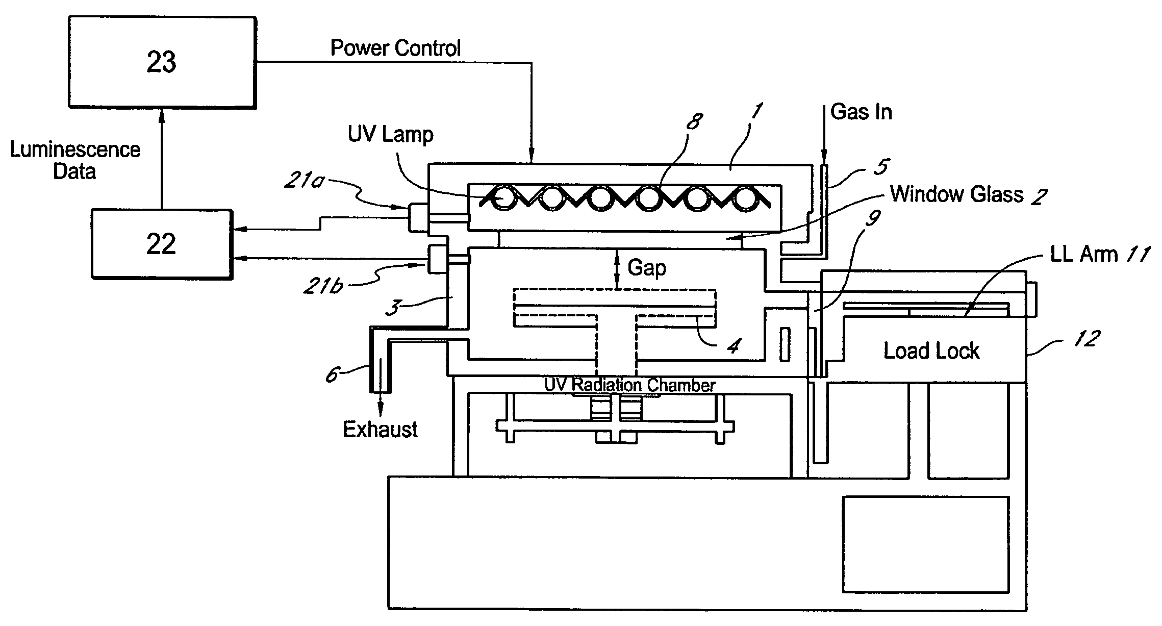
[0027]In an embodiment of the present invention, a method for managing UV irradiation for curing a semiconductor substrate, may comprise: (a) passing UV light through a transmission glass window provided in a chamber for curing a semiconductor substrate placed in the chamber; (b) monitoring an illuminance upstream of the transmission glass window and an illuminance downstream of the transmission glass window; and (c) determining a timing and / or duration of cleaning of the transmission glass window, a timing of replacing the transmission glass window, a timing of replacing a UV lamp, and / or an output of the UV light based on the monitored illuminances.

[0028]In the above, in an embodiment, the monitoring step may comprise measuring the illuminance upstream of the transmission glass window by an illuminometer...


PUM


Abstract

A method for managing UV irradiation for curing a semiconductor substrate, includes: passing UV light through a transmission glass window provided in a chamber for curing a semiconductor substrate placed in the chamber; monitoring an illuminance upstream of the transmission glass window and an illuminance downstream of the transmission glass window; determining a timing and / or duration of cleaning of the transmission glass window, a timing of replacing the transmission glass window, a timing of replacing a UV lamp, and / or an output of the UV light based on the monitored illuminances.

Description

BACKGROUND OF THE INVENTION[0001]1. Field of the Invention[0002]The present invention generally relates to a method for controlling UV irradiation for curing a semiconductor substrate and a method for processing a semiconductor substrate using the UV irradiation controlling method.[0003]2. Description of the Related Art[0004]Traditionally, UV processing apparatuses have been commonly used for the modification of various processing targets with UV light and the production of substances by means of photochemical reaction. The recent trend of higher integration of devices results in increasingly finer wiring designs and multi-layer wiring structures, which gives rises to a need to reduce the interlayer volume in order to increase the device speed while reducing the power consumptions. To reduce the interlayer volume, low-k (low dielectric constant film) materials are used. However, use of a low-k material results in lower mechanical strength (indicated by elastic modulus, or EM) as the...

Claims


Application Information

Patent Timeline
Patent Type & Authority Patents(United States)
IPC IPC(8): H01L21/66
CPCH01L21/67115H01L21/67253
Inventor MATSUSHITA, KIYOHIROKAGAMI, KENICHI
Owner ASM JAPAN
Why Eureka
Try Eureka