Analog-to-digital converter operable with staggered timing

an analog-to-digital converter and time-interleave technology, applied in the field of time-interleaved analog-to-digital converters, can solve the problems of affecting the xout of the conversion error, the increase in the number of time offset problems, and the inability to adjust the output spectrum correctly, so as to reduce the incorrect adaptation of the output spectrum and reduce the level of circuit complexity. , the effect of low additional cos

Inactive Publication Date: 2009-03-10
INFINEON TECH AG
View PDF12 Cites 19 Cited by
  • Summary
  • Abstract
  • Description
  • Claims
  • Application Information

AI Technical Summary

Benefits of technology

[0028]One advantage of the present invention may also be that a very low level of circuit complexity is necessary to reduce the incorrect adaptation in the output spectrum. In particular, the circuit complexity which results for the reduction of the incorrect adaptation is restricted to a connection network which can be configured at least once in order to implement the respective optimum converter sequence. In particular even when there is an increasing number of parallel individual analog-to-digital converters, the additional cost is low. All that is necessary here is a small amount of additional expenditure on sorting the individual analog-to-digital converters.
[0029]In this way the present invention is independent of the absolute precision of an identification algorithm such as is performed in known approaches to solutions which are acknowledged at the beginning. Although the present invention, accepts a certain degree of incorrect adaptation, the expenditure on circuitry and the computational complexity for reducing the incorrect adaptation is reduced greatly compared to previous approaches to solutions. As a result, the circuit arrangement according to the invention is very economical in terms of power but at the same time supplies a very precise conversion result.
[0030]In a first version of the inventive converter, the connection network has at least a clock input into which at least a clock signal can be input. The connection network generates, from the input clock signals, clocked control signals which have a predetermined time difference with respect to one another and are used to actuate the individual analog-to-digital converters.
[0031]In a second version of the inventive converter, at least three, preferably at least four individual analog-to-digital converters are provided which are each connected by their signal path to an input of the converter arrangement in order to pick-up an analogue input signal present at the input, sample the picked-up input signal and convert it into digital intermediate signals. The invention is particularly advantageous and effective in art analog-to-digital converter with a very large number of individual analog-to-digital converters such as, for example, 128 or 256 individual analog-to-digital converters within one converter array.
[0032]A filter may be connected downstream of the converter arrangement and filters the output signal in order to filter out the energy from undesired interference spectrums, present in addition to the useful spectrum, from the spectrum of the output signal. A low-pass filter is preferably provided as a filter for low-pass filtering.
[0033]In third version of the inventive converter, the connection network has a counter which is triggered by a central clock signal and which generates a counter sequence. Each individual analog-to-digital converter has connected in front of it at the control end at least an actuation circuit which assigns in each case one counter reading of the counter sequence generated by the counter to each individual analog-to-digital converter. The actuation circuit may in each case have a memory register and a comparator, with the comparator being configured to compare the counter sequence with a register content which is stored in, the memory register.

Problems solved by technology

However, with such an array of individual ADCs 2-1 to 2-N there is a problem that any type of incorrect adaptation (mismatch) of the individual ADCs 2-1 to 2-N to one another leads to a conversion error which affects the output signal XOUT.
Especially at high frequencies, the intervals or timing differences of adjacent converters become smaller and smaller so that the time offset problem becomes more and more pronounced here.
In the same way, differences in the amplification of the input signal lead to undesired additional spectrums whose frequency is however dependent on the input signal.
Incorrect adaptations in the bandwidth of the individual parallel ADCs of the converter array typically give rise to undesired additional interference spectrums.
In particular, any form of deviation in the transmission behaviour and thus in the transmission function of the individual AD leads to additional undesired interference spectrums in the output signal.
However, this is undesired, in particular if the power of these additional spectrums 7 in the region of the input spectrum 6 is very large.
The problem of incorrect adaptation, and in particular the incorrect adaptation resulting from different time offset values increases with increasingly small structure sizes such as are used in future manufacturing technologies in what is referred to as the deep submicron range with structure widths of less than 70 nm since absolute errors have increasingly serious effects there owing to the smaller structural widths.
Analogue circuit measures for reducing incorrect adaptations entail a very high level of complexity of circuitry together with a very high power consumption, if such a reduction is at all possible, in particular when there are a plurality of individual ADCs of one converter array.
In particular at very high frequencies this solution is however very difficult to implement at acceptable cost.
In order to determine and thus also correct sampling time error adaptations there are currently only very costly numeric methods which are capable of being implemented with an exorbitantly high computational complexity, which far exceeds acceptable limits, in particular when a plurality of individual ADCs of one TIADC are used.
Above all, the correction which has to take place during the ongoing operation of the TIADC constitutes a hurdle which is frequently impossible to overcome technically owing to the necessary computing power therefor.
For this reason, this method of error compensation is frequently not practical.
This introduced randomness in the sequence of the individual ADCs brings about the uniform distribution of the spectral power arising over the entire frequency band due to incorrect adaptations.
However, a problem with these methods is that there is no effective improvement achieved in the signal-to-noise ratio since the undesired power is in fact not eliminated but merely distributed uniformly.
For this reason, with such short signals there is usually insufficient stochastic distribution of the converters.
Moreover, with this randomization method there are also certain restrictions which result from the physical peripheral conditions of the operation of the converter (setup and hold times).

Method used


Image

  • Analog-to-digital converter operable with staggered timing
  • Analog-to-digital converter operable with staggered timing
  • Analog-to-digital converter operable with staggered timing

Examples


Embodiment Construction

[0054]Identical or functionally identical elements and signals are referred to with the same reference symbols in the figures of the drawing unless stated otherwise.

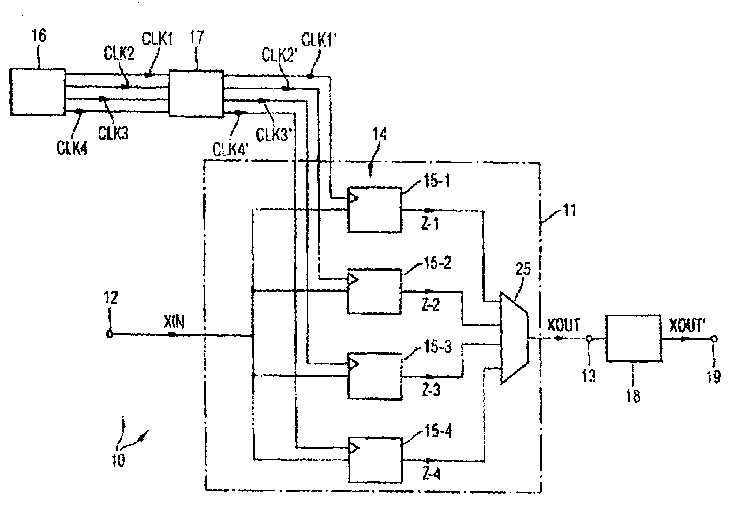
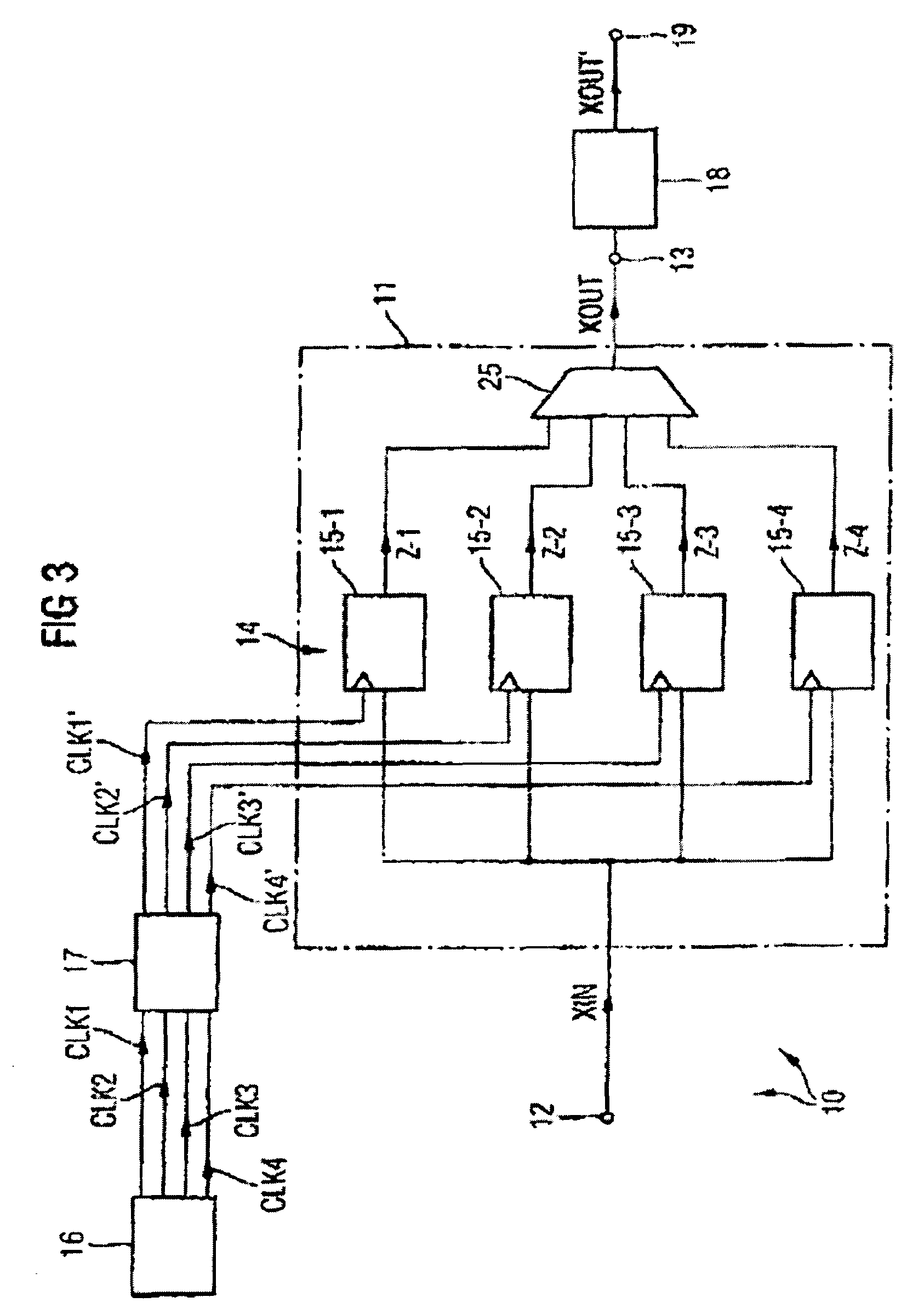
[0055]In FIG. 3, the circuit arrangement according to the invention is referred to by reference symbol 10. The circuit arrangement 10 contains a time interleaved analog-to-digital converter 11 which is connected at the input side to an input terminal 12 and at the output side to an output terminal 13. The analog-to-digital converter 11 has a converter array 14 which is composed in the present exemplary embodiment of four individual analog-to-digital converters 15-1 to 15-4 which are also referred to below as ADC channels 15-1 to 15-4. In FIG. 3, N=4 is therefore true. The individual analog-to-digital / convertors 15-1 to 15-4 are arranged in parallel with one another in the present exemplary embodiment, that is to say they are each connected at the input ends to the input 12 and at the output ends to the output 13 via a mu...


PUM


Abstract

An arrangement for a time interleaved analog-to-digital converter that converts an signal to a digital signal and has a converter array with a plurality of analog-to-digital converters arranged in a fixed sequence in parallel with one another and can be operated with staggered timing with respect to one another is disclosed. The arrangement has a connection network which, for the purposes of actuation with staggered timing, generates in each case one control signal for an individual analog-to-digital converter in each case, with the connection network predefining the time sequence with which the control signals actuate the individual analog-to-digital converters in such a way that owing to this sequence of the control signals and thus the sequence of the actuated individual analog-to-digital converters there is at least a reduction in an interference spectrum in the spectrum of the input and / or output signal. A sorting method for operating this analog-to-digital converter is also disclosed.

Description

PRIORITY AND CROSS REFERENCE TO RELATED APPLICATION[0001]This application claims priority to German Patent Application No. 10 2004 049 161.5, filed Oct. 8, 2004, which is incorporated by reference herein in its entirety.BACKGROUND OF THE INVENTION[0002]1. Field of the Invention[0003]The invention relates to a time interleaved analog-to-digital converter, and to a sorting method for operating this analog-to-digital converter.[0004]2. Description of the Related Art[0005]In modern data processing there is a need to process increasingly large amounts of data in shorter and shorter times and to condition it for further data communication. The respective electronic components, for example memory modules, processors and also logic components, such as PLDs or FPGAs, are therefore configured for increasingly high clock frequencies. As a result of this the analog-to-digital converters (ADC) which are present in such electronic components have correspondingly high sampling rates.[0006]An analo...

Claims


Application Information

Patent Timeline
Patent Type & Authority Patents(United States)
IPC IPC(8): H03M1/00
CPCH03M1/1215
Inventor DRAXELMAYR, DIETERKUBIN, GERNOTVOGEL, CHRISTIAN
Owner INFINEON TECH AG
Why Eureka
Try Eureka