Hole-trapping materials for improved OLED efficiency

a technology of oled efficiency and hole trapping, which is applied in the direction of discharge tube luminescnet screen, other domestic articles, natural mineral layered products, etc., can solve the problems of insufficient el efficiency, insufficient luminous efficiency, and limiting the competitiveness of oled applications, so as to improve the luminance yield and improve the color coordinates

Active Publication Date: 2009-03-17
GLOBAL OLED TECH
View PDF20 Cites 52 Cited by
  • Summary
  • Abstract
  • Description
  • Claims
  • Application Information

AI Technical Summary

Benefits of technology

[0007]It is an object of the present invention to provide efficient OLED devices producing visible light with significantly improved luminance yield and improved color coordinates.

Problems solved by technology

Luminous efficiency of OLED devices remains a factor limiting possible OLED applications and competitiveness.
Although EL efficiency and color have been improved significantly using doped light-emitting layers of various compositions, the problem of insufficient EL efficiency persists.
Insufficient luminous efficiency presents an obstacle for many desirable practical applications.

Method used


Image

  • Hole-trapping materials for improved OLED efficiency
  • Hole-trapping materials for improved OLED efficiency
  • Hole-trapping materials for improved OLED efficiency

Examples


##ventive examples 1-5

COMPARATIVE AND INVENTIVE EXAMPLES 1-5

Efficiency-improving Effect of the Hole-trapping Material on Electroluminescence of Blue OLEDS

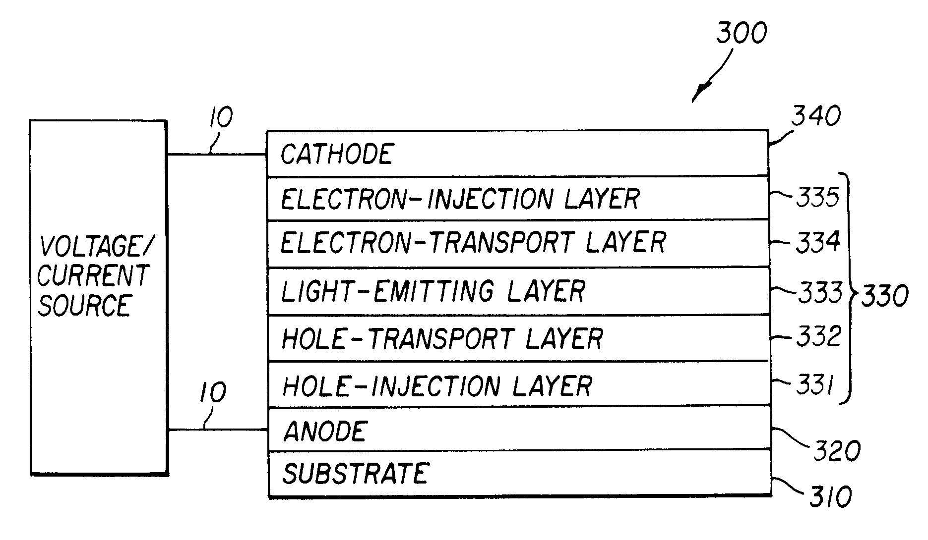
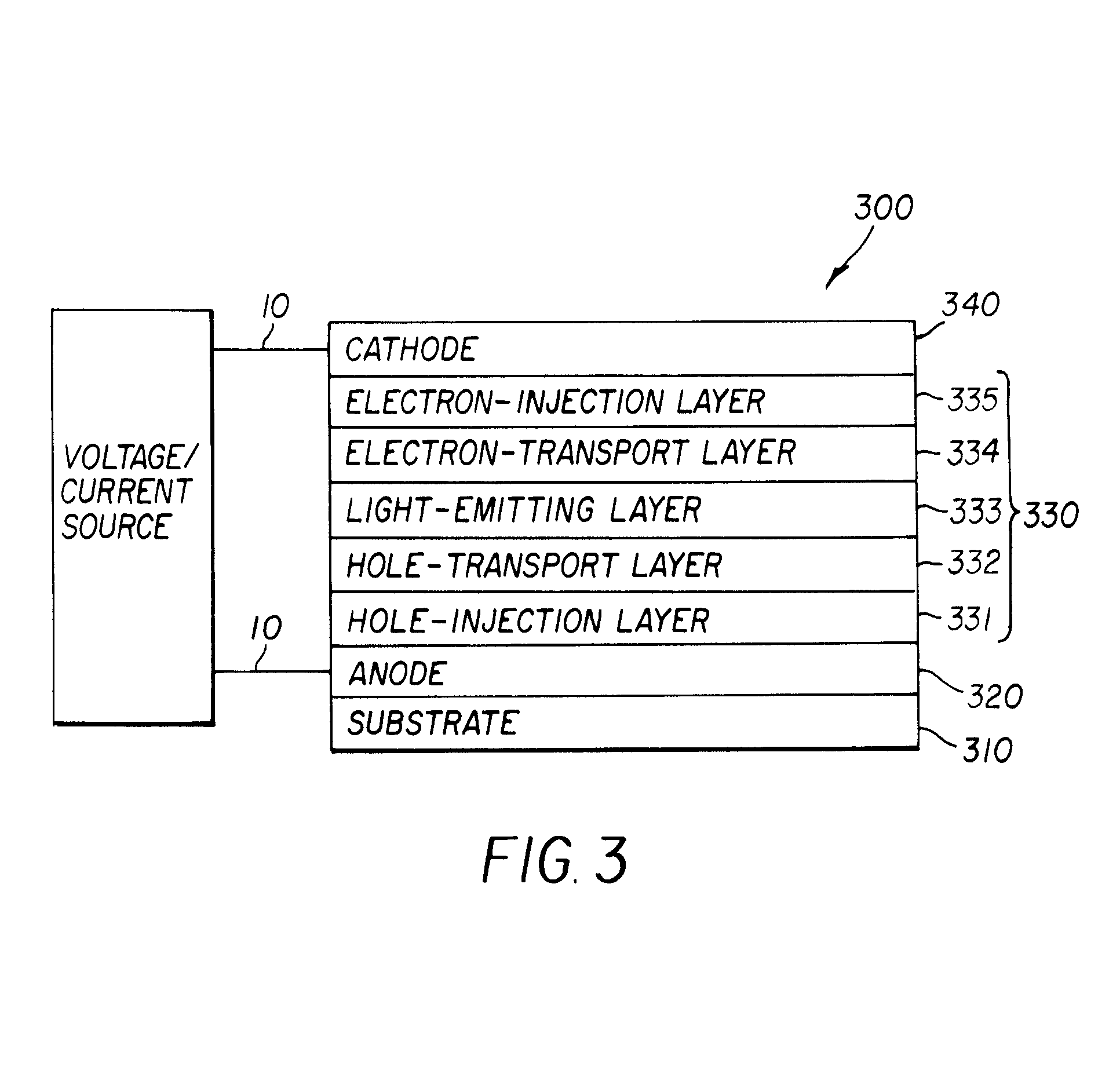
[0384]OLED devices were prepared as follows. A glass substrate coated with about 850 Å transparent indium-tin-oxide (ITO) conductive layer was cleaned and dried using a commercial glass scrubber tool. The ITO surface was subsequently treated with an oxidative plasma to condition the surface as an anode. Over the ITO was deposited a 10 Å thick hole-injecting layer of fluorocarbon (CFx) by plasma-assisted deposition of CHF3. The following layers were deposited in the following sequence by sublimation from heated crucible boats in a conventional vacuum deposition chamber under a vacuum of approximately 10−6 Torr: (1) a hole-transport layer, 750 Å thick, including NPB; (2) a light-emitting layer, 400 Å thick, including host and dopant and the hole-trapping material in certain ratio (indicated in Tables 1-3); (3) an 200 Å electron-transport layer, including ...

##ventive examples 6-8

COMPARATIVE AND INVENTIVE EXAMPLES 6-8

Efficiency-improving Effect of the Hole-trapping Material on Electroluminescence of Blue OLEDs Containing Lithium Dopant in the Electron-transporting Layer

[0389]For layer thicknesses and concentrations of materials in multi-component layers of each device see Table 2. OLED devices were prepared similar to Examples 1-5 except the electron-transporting layer AlQ3 was doped with alkali metal, lithium, in the 1:1 molar ratio.

[0390]The EL characteristics of these devices are given in Table 2.

[0391]As can be seen from Table 2, Inventive Examples 6-8 demonstrate addition of the hole-trapping material at concentration of less than 5% results in the electroluminescence efficiency improvement of greater than 2 times than that of comparative devices for devices containing a variety of hosts with the dopant Blue 2 and lithium doping of the electron-transporting layer.

[0392]

TABLE 2Comparative and inventive examples:Efficiency,W / A at 20λmaxW / A vs J@20 mA / cm2,...

##ventive examples 9 and 10

COMPARATIVE AND INVENTIVE EXAMPLES 9 AND 10

Efficiency-improving Effect of the Hole-trapping Material on Electroluminescence of Blue-Green OLEDs Containing Blue-Green 2 Dopant

[0393]For layer thicknesses and concentrations of materials in multi-component layers of each device see Table 3. OLED devices were prepared similar to Examples 1-5 except that in place of the blue dopants the light-emitting layer contained 1-5% dopant Blue-Green 2.

[0394]The EL characteristics of these devices are given in Table 3.

[0395]As can be seen from Table 3, Inventive Examples 9 and 10 demonstrate addition of the hole-trapping material at concentration of less than 5% results in the device luminance efficiencies improvement to 0.10-0.11 W / A. Moreover, a thicker light-emitting layer comprising hole-trapping material, host, and dopant followed by an electron-transporting layer with added alkali metal dopant can provide 0.134 W / A (12.4 cd / A) at color coordinates of 0.16, 0.39 and a lifetime of 1,200 h at roo...


PUM

PropertyMeasurementUnit
current efficiencyaaaaaaaaaa
thicknessaaaaaaaaaa
thicknessaaaaaaaaaa

Abstract

An organic light-emitting device includes a light-emitting layer including a host, a dopant, and a hole-trapping material, wherein the hole-trapping material is provided at 0.01 to less than 5% by volume relative to the light-emitting layer volume, has an oxidation potential that is selected so that it is less than the oxidation potential of the host in order to serve as a hole trap, has an oxidation potential that is selected so as to avoid formation of a certain charge transfer complex between the hole-trapping material and the host if the charge transfer complex causes a reduction in the electroluminescent efficiency of the dopant, and has an oxidation potential that is selected so as to avoid formation of the charge transfer complex between the hole-trapping material and the dopant.

Description

FIELD OF THE INVENTION[0001]This invention relates to an electroluminescent (EL) device comprising a light-emitting layer including a host, a dopant, and a hole-trapping material providing improved electroluminescent efficiency and color.BACKGROUND OF THE INVENTION[0002]Organic light-emitting diodes (OLED), also known as organic electroluminescent (EL) devices, are a class of electronic devices that emit light in response to an electrical current applied to the device. The structure of an OLED device generally includes an anode, an organic EL medium, and a cathode. The term organic EL medium herein refers to organic materials or layers of organic materials disposed between the anode and the cathode in the OLED device. The organic EL medium can include low molecular weight compounds, high molecular weight polymers, oligomers of low molecular weight compounds, or biomaterials in the form of a thin film or a bulk solid. The medium can be amorphous or crystalline. Organic electrolumines...

Claims


Application Information

Patent Timeline
Patent Type & Authority Patents(United States)
IPC IPC(8): H01L51/50
CPCC09K11/06H01L51/5012H05B33/14C09K2211/1011C09K2211/1029C09K2211/1055C09K2211/1088H01L51/005Y10S428/917H01L51/0071H01L51/008H01L51/0081Y10T428/24942H01L51/0054H10K85/60H10K85/622H10K85/322H10K85/657H10K85/324H10K50/11
Inventor JARIKOV, VIKTOR V.
Owner GLOBAL OLED TECH
Why Eureka
Try Eureka