Semiconductor acceleration sensor device and fabrication method thereof

a technology of acceleration sensor and semiconductor, applied in the direction of acceleration measurement using interia force, solid-state device, instruments, etc., can solve the problems of acceleration not being detected accurately, affecting piezoelements, and dimensional change in horizontal direction, so as to suppress the distortion generated on the acceleration sensor chip by temperature change, improve the detection accuracy of acceleration sensor, and suppress the effect of horizontal direction dimensional chang

Inactive Publication Date: 2009-04-07
LAPIS SEMICON CO LTD
View PDF4 Cites 16 Cited by
  • Summary
  • Abstract
  • Description
  • Claims
  • Application Information

AI Technical Summary

Benefits of technology

[0012]Since the low elasticity element is filled in the concave section, the dimensional change of the low elasticity element when the ambient temperature changes occurs mainly in the vertical direction, and the dimensional change in the horizontal direction can be suppressed. In other words, the distortion generated on the acceleration sensor chip by the temperature change is suppressed. Therefore, the detection accuracy of the acceleration sensor can be improved.

Problems solved by technology

As a result, distortion is generated in the acceleration sensor chip if the ambient temperature changes.
If distortion is generated in the acceleration sensor chip, the piezoelements are affected.
In other words, acceleration cannot be detected accurately if the temperature changes.

Method used


Image

  • Semiconductor acceleration sensor device and fabrication method thereof
  • Semiconductor acceleration sensor device and fabrication method thereof
  • Semiconductor acceleration sensor device and fabrication method thereof

Examples


first embodiment

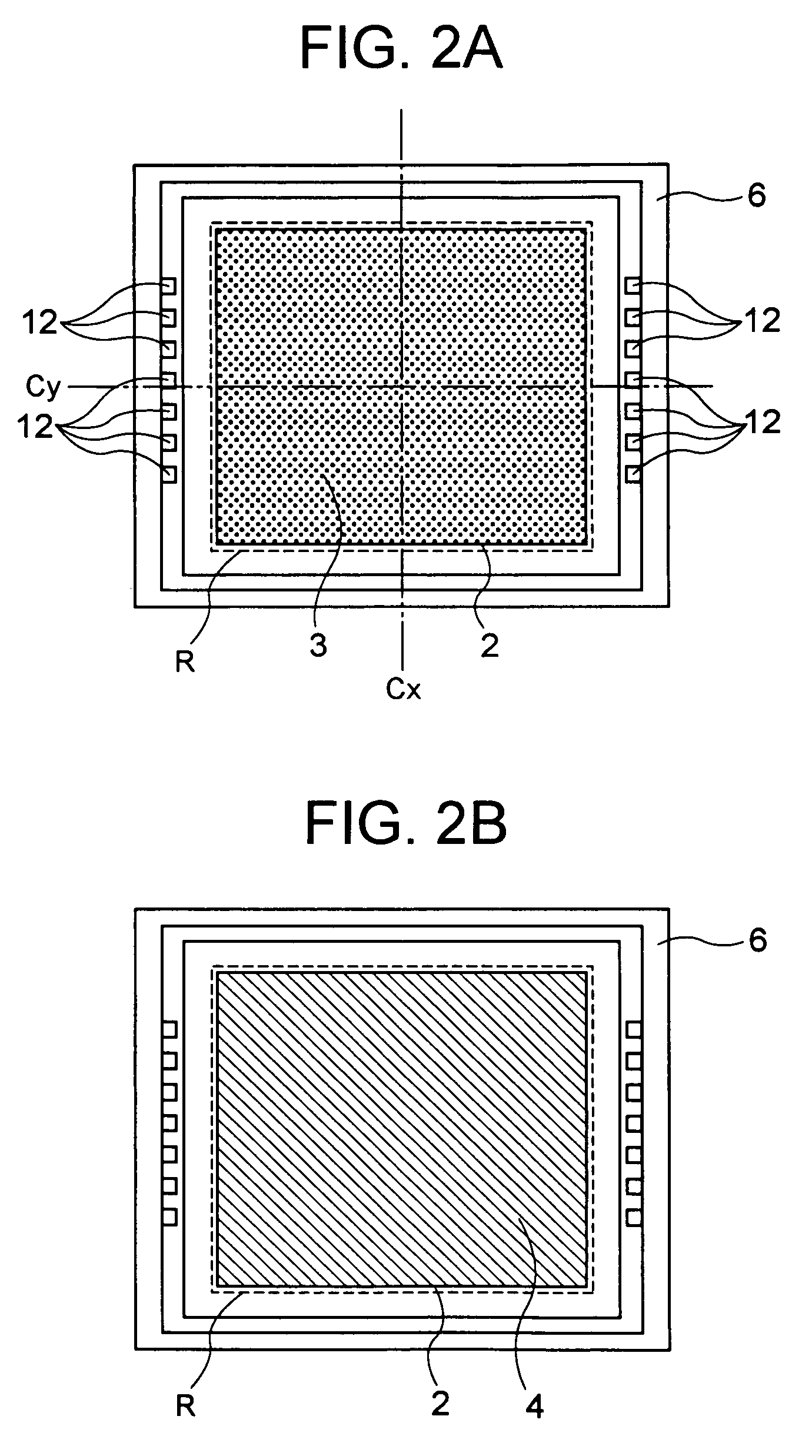
[0043]The structure and fabrication method of the semiconductor acceleration sensor device according to the first embodiment of the present invention will be described with reference to FIG. 1A through FIG. 4E. FIG. 3A and FIG. 3B show examples when the shape, size and position of the low elasticity element 3 are different from those of the low elasticity element 3 shown in FIG. 2A.

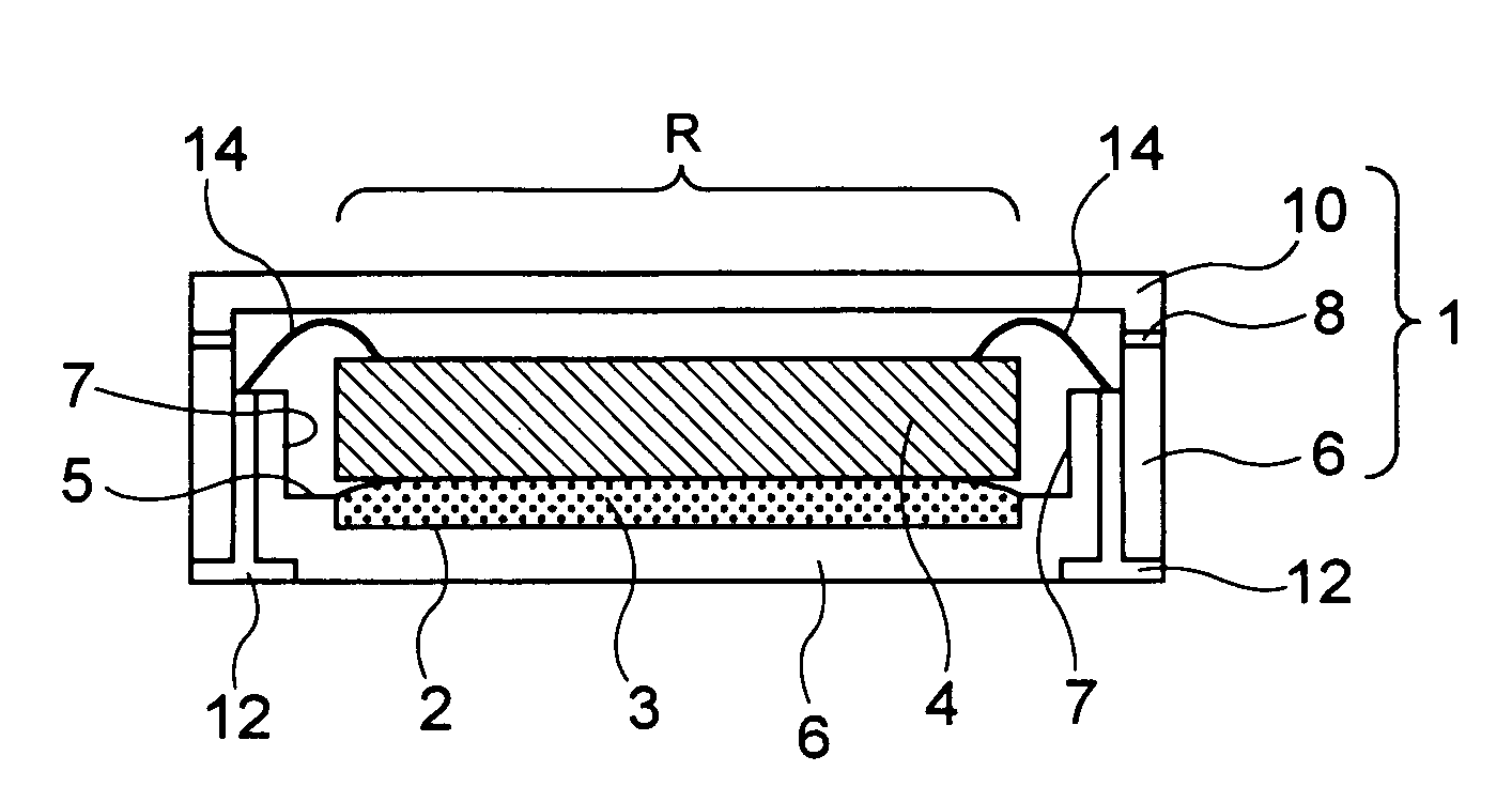
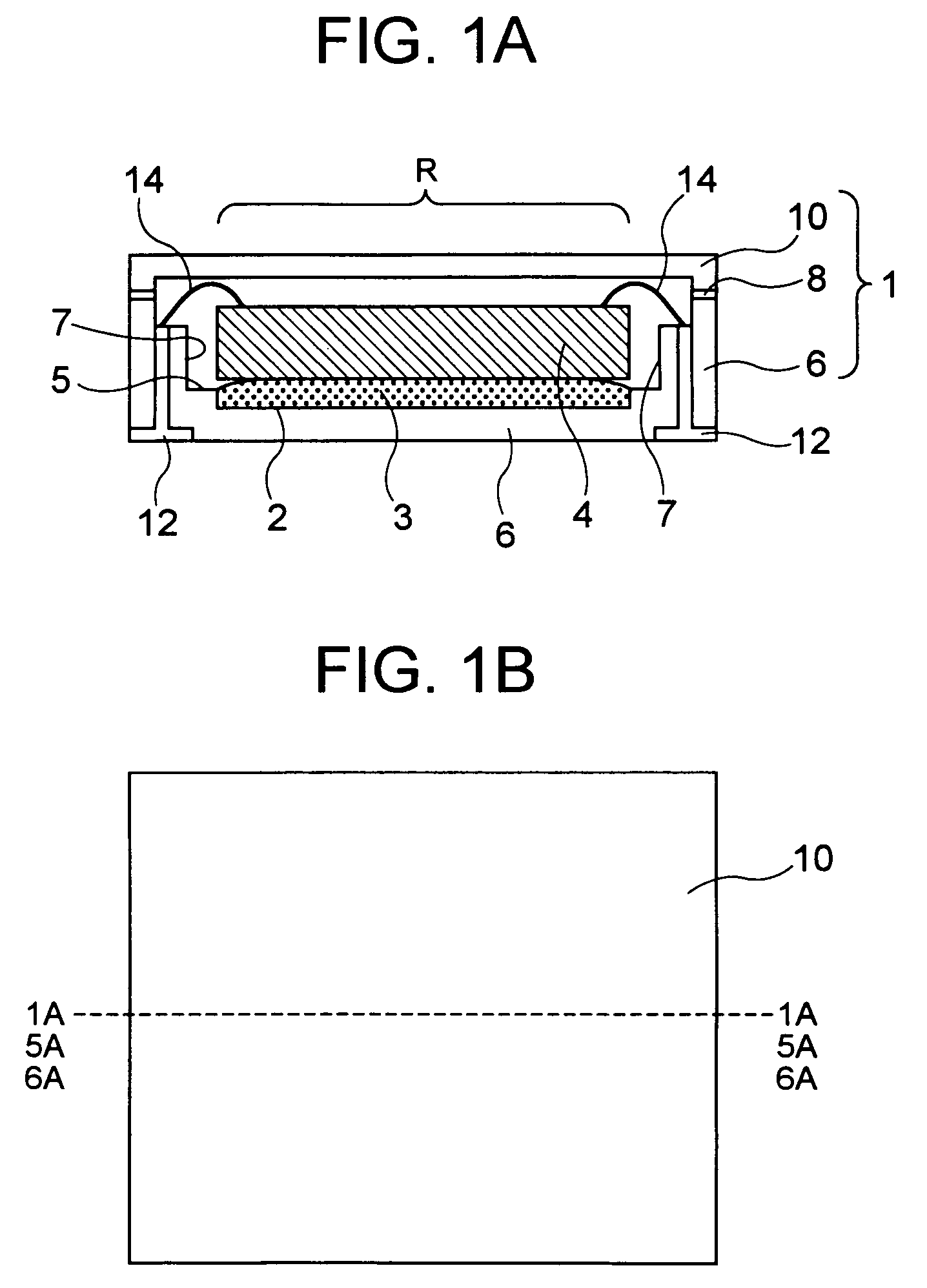
[0044]Referring to FIG. 1A, the acceleration sensor chip 4 for generating electric signals according to the magnitude and direction of the applied acceleration is housed inside the hollow package 1. The package 1 includes the chip housing section 6 made of ceramic and the top cover 10 made of ceramic. The top cover 10 is placed over the chip housing section 6. The top cover 10 is fixed to the chip housing section 6 by adhesive 8 to cover (close) the chip housing section 6. The acceleration sensor chip 4, housed inside the package 1, is sealed in by the package 1. In the chip housing section 6, a plurality...

second embodiment

[0089]The structure and fabrication method of the semiconductor acceleration sensor device according to the second embodiment of the present invention will now be described with reference to FIG. 7A through FIG. 9B and FIG. 4A through FIG. 4E. Description of the second embodiment which is the same as that of the structure and fabrication method of the semiconductor acceleration sensor device according to the first embodiment will be omitted.

[0090]FIG. 7B is a plan view of the semiconductor acceleration sensor device of the second embodiment. FIG. 7A is a cross-sectional view of the semiconductor acceleration sensor device of the second embodiment, taken along the line 7A-7A in FIG. 7B. FIG. 8A is a plan view depicting the semiconductor acceleration sensor device of the second embodiment when the top cover 10, adhesive 8, wires 14 and acceleration sensor chip 4 are removed. FIG. 8B is a plan view depicting the acceleration sensor chip 4 mounted on the low elasticity element 3 in FIG....

third embodiment

[0097]The structure and fabrication method of the semiconductor acceleration sensor device according to the third embodiment of the present invention will now be described with reference to FIG. 10A through FIG. 12B and FIG. 4A through FIG. 4E. Description of the third embodiment which is the same as that of the structure and fabrication method of the semiconductor acceleration sensor device according to the first embodiment will be omitted.

[0098]FIG. 10B is a plan view depicting the semiconductor acceleration sensor device of the third embodiment. FIG. 10A is a cross-sectional view of the semiconductor acceleration sensor device of the third embodiment, taken along the line 10A-10A in FIG. 10B. FIG. 11A is a plan view depicting the semiconductor acceleration sensor device of the third embodiment when the top cover 10, adhesive 8, wires 14 and acceleration sensor chip 4 are removed. FIG. 11B is a plan view depicting the acceleration sensor chip 4 mounted on the low elasticity elemen...


PUM


Abstract

A semiconductor acceleration sensor device has an acceleration sensor chip and a hollow package to house the acceleration sensor chip. A concave section is formed in a predetermined area on a bottom face inside the package. The semiconductor acceleration sensor device also has a low elasticity element with adhesiveness. The low elasticity element is filled in the concave section. The acceleration sensor chip is mounted on the low elasticity element. The adhesive surface between the low elasticity element and the acceleration sensor chip is higher than the bottom face.

Description

BACKGROUND OF THE INVENTION[0001]1. Field of the Invention[0002]The present invention relates to a semiconductor acceleration sensor device having an acceleration sensor chip mounted on a package.[0003]2. Description of the Related Art[0004]A typical conventional semiconductor acceleration device has an acceleration sensor chip for outputting an electric signal in accordance with a magnitude and direction of applied acceleration, and the acceleration sensor chip is mounted on a package. Various types of semiconductor acceleration sensor devices have been known in the art. One example is a semiconductor acceleration sensor device having the structure shown in FIG. 17 of the accompanying drawings. In this semiconductor acceleration sensor device, the acceleration sensor chip 4′ shown in FIG. 16 of the accompanying drawings is mounted on the package 1′. This conventional acceleration sensor device will be described with reference to FIG. 16 and FIG. 17.[0005]The acceleration sensor chi...

Claims


Application Information

Patent Timeline
Patent Type & Authority Patents(United States)
IPC IPC(8): G01P15/125
CPCG01P1/023G01P15/0802H01L2224/32225H01L2224/83385H01L2224/73265H01L2924/15153H01L2924/16195G01P15/08
Inventor INO, YOSHIHIKO
Owner LAPIS SEMICON CO LTD
Why Eureka
Try Eureka