Printed wiring board manufacturing apparatus, printed wiring board, method for manufacturing printed wiring board, and electronic device

A technology for printed wiring boards and manufacturing devices, which is applied in the field of electronic equipment for printed wiring boards, and can solve the problems of reduced surface area, poor space efficiency, and high manufacturing costs of printed wiring boards 510

Inactive Publication Date: 2008-05-28
SHARP KK
View PDF3 Cites 6 Cited by
  • Summary
  • Abstract
  • Description
  • Claims
  • Application Information

AI Technical Summary

Problems solved by technology

Since the printed wiring board 510 cannot be bent, it cannot be formed into a shape having a width greater than the cylinder diameter
[0010] Therefore, since the maximum width is limited to the size of the diameter, the surface area of ​​the printed wiring board 510 itself is also reduced, so there is a problem that it is difficult to increase the mounting density of components.
In addition, since the arrangement position of the printed wiring board 510 is limited, the space efficiency is very bad, and there is a problem that it is difficult to miniaturize the electronic device 500.
[0011] Although it is also conceivable that the printed wiring board 510 can be used as long as it is formed as a flexible wiring board and bent along the inner wall surface of the housing 501, there is actually a problem that the flexible printed wiring board body is made in a flat shape, Bending in areas such as through-holes and component mounting lands may lead to disconnection or delamination between laminated layers, and it is unrealistic to bend to follow the shape of the case 501.
[0015] However, since the rigid printed wiring board with flexibility must form the hard part 520a and the flexible part 520b, there are problems of complicated structure and high manufacturing cost.
In addition, there is a problem that only the hard part 520a can be mounted with components, and it is actually difficult to increase the surface area that can be used for mounting components.
For example, injection molding metal molds are expensive, and the formation of three-dimensional molded substrates and the formation of wiring patterns also require considerable effort.
In addition, at the same time, due to the large restrictions caused by the applicable materials and manufacturing methods, it is difficult to achieve high density, high precision, and high reliability like ordinary printed wiring boards.
[0018] In addition, the problem of general printed wiring board manufacturing equipment is that, represented by etching and plating production lines, the manufacturing equipment is relatively large, especially its length is long, often reaching tens of meters, and the factory occupies a large area.

Method used


Image

  • Printed wiring board manufacturing apparatus, printed wiring board, method for manufacturing printed wiring board, and electronic device
  • Printed wiring board manufacturing apparatus, printed wiring board, method for manufacturing printed wiring board, and electronic device
  • Printed wiring board manufacturing apparatus, printed wiring board, method for manufacturing printed wiring board, and electronic device

Examples


Embodiment Construction

[0171] Embodiments of the present invention will be described below with reference to the drawings.

[0172]

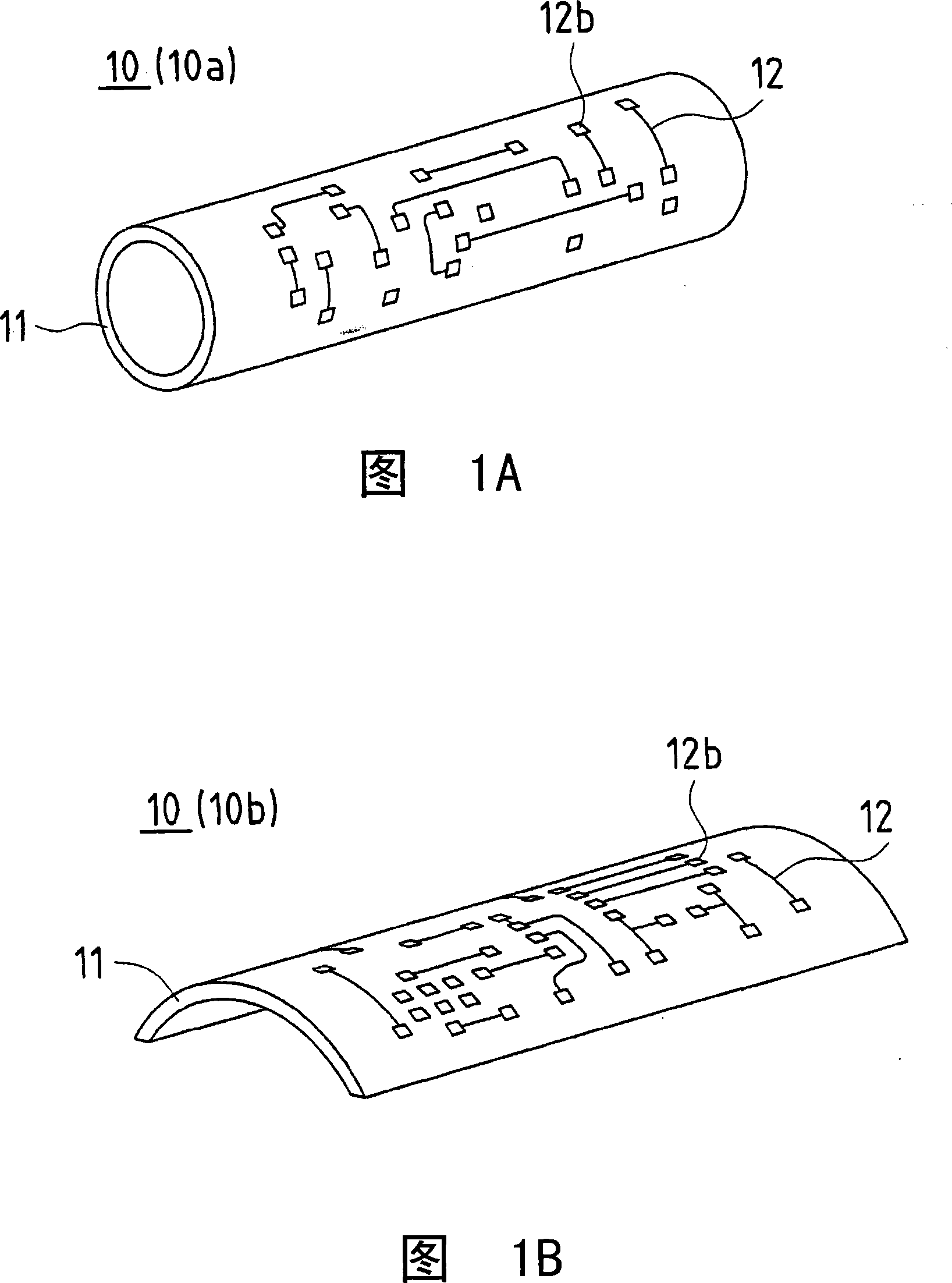
[0173] 1A and 1B are schematic perspective views showing a printed wiring board according to Embodiment 1 of the present invention. FIG. 1A shows a cylindrical insulating substrate (printed wiring board), and FIG. 1B shows a curved arc-shaped substrate. In the case of an insulating substrate (printed wiring board).

[0174] A printed wiring board 10 according to this embodiment includes: a curved insulating substrate 11 as a wiring substrate; and a wiring pattern 12 formed by a conductor layer formed on the insulating substrate 1 . The wiring pattern 12 has a component mounting land portion 12b in a bent region of the insulating substrate 11 .

[0175] That is, the printed wiring board 10 related to the present embodiment is a printed wiring board in which the wiring pattern 12 having the land portion 12b for component mounting is formed on the insulating substrate...


PUM


Abstract

According to an embodiment of the present invention, a printed wiring board manufacturing apparatus being provided with a drum unit having a processing cylinder that holds the printed wiring board material and comprises a cylinder outer circumference and a processing unit that performs processing on the printed wiring board material held by the processing cylinder.

Description

technical field [0001] This application claims priority based on Japanese Patent Application No. 2006-313331 filed on November 20, 2006 in Japan. Accordingly, all content thereof is included in this application. [0002] The present invention relates to a printed wiring manufacturing apparatus for manufacturing a printed wiring board with a curved insulating substrate by using a cylindrical body for processing with a cylindrical outer periphery, a printed wiring board with a curved insulating substrate, and a printed wiring board for manufacturing a curved insulating substrate. A method of manufacturing a printed wiring board with an insulating substrate, and an electronic device mounted with a printed wiring board having a curved insulating substrate. Background technique [0003] Printed wiring boards used in electronic equipment are generally flat. This is because most electronic equipment is formed in a box shape, and the shape of the printed wiring board installed ins...

Claims


Application Information

Patent Timeline
Patent Type & Authority Applications(China)
IPC IPC(8): H05K3/00H05K3/06H05K3/42
CPCH05K2203/013H05K3/4652B32B38/145H05K3/0082H05K2201/09018H05K1/0393B32B2037/243B32B2309/68H05K2203/107B32B2037/109H05K2203/1105H05K3/187H05K2203/0285B32B2457/08H05K2203/095H05K3/241H05K3/125B32B38/0004H05K2203/0165B32B2310/0843B32B37/0046H05K3/064H05K3/0052H05K2203/0134Y10T428/13
Inventor 上野幸宏
Owner SHARP KK
Why Eureka
Try Eureka