Surface mount poke in connector

a technology of surface mount and electrical connector, which is applied in the direction of connecting devices, sustainable manufacturing/processing, and contact members penetrating/cutting insulation/cable strands, etc. it can solve the problems of time-consuming and costly steps of soldering wire leads to boards, and achieve the effect of reducing the shadowing of connectors in the low profile of the connector

Active Publication Date: 2009-04-07
TYCO ELECTRONICS LOGISTICS AG (CH)
View PDF33 Cites 47 Cited by
  • Summary
  • Abstract
  • Description
  • Claims
  • Application Information

AI Technical Summary

Benefits of technology

[0008]This invention provides for a low profile surface mounted electrical connector (SMEC) for connecting a wire lead to a printed circuit board (PCB) or other suitable component surface. The low profile of the connector reduces shadowing by the connector when mounted on a PCB supporting LEDs. The SMEC is attached to the PCB by surface mount technology (SMT), a standardized automated process for placing and attaching electrical and electronic components to PCBs. Attachment may be by soldering, using a conductive adhesive, or other similar method.
[0013]In an alternative embodiment, the housing is omitted from the SMEC and the contact is left uncovered upon the PCB surface. This alternative embodiment may be used to reduce the cost of the connection.
[0014]The housing may be formed of a high temperature material that is lightweight and high strength, and able to operate in a high temperature environment such as along the surface of a PCB that supports LEDs. The housing may be formed of a high temperature liquid crystalline polymer (LCP) such as Zenite 6330® by E.I. du Pont de Nemours and Company of Wilmington, Del. or a high temperature nylon such as Stanyl 46 HF® by DSM Engineering Plastics North America, Inc., based in Reading, Pa., or any other known industry acceptable non-conductive high temperature resin. The housing is designed with a low profile and small footprint so that it may be placed upon a PCB supporting lighting LEDs without shadowing or blocking the light emissions of the LEDs. The housing at least partially covers the contact.
[0016]The first step in forming the contact is to stamp, cut or by other similar shaping methods form a predetermined shape from stock material. Then, a forming of the predetermined shape into the contact with extended attachment points may be performed by any material shaping method such as rolling and working to form the desired shape. The desired shape may be cylindrical, rectangular, square of other geometry. A combination of different shaping techniques may be used to complete the contact design. The extended attachment points of the contact may be provided with an edge bevel to assist in solder reflow during attachment to the PCB. Beveling of the attachment points is most important when pre-plated stock material is used, but the barrel may be plated at any point during the contact forming process.

Problems solved by technology

SMT allows for mounting electrical devices on both sides of a PCB, which was not possible using through hole mounting technology.
The step of soldering the wire leads to the boards is time consuming and costly.

Method used


Image

  • Surface mount poke in connector
  • Surface mount poke in connector
  • Surface mount poke in connector

Examples


Embodiment Construction

[0025]The present invention now will be described more fully hereinafter with reference to the accompanying drawing, in which a preferred embodiment of the invention is shown. This invention may, however, be embodied in many different forms and should not be construed as limited to the embodiments set forth herein; rather, these embodiments are provided so that this disclosure will be thorough and complete and will fully convey the scope of the invention to those skilled in the art.

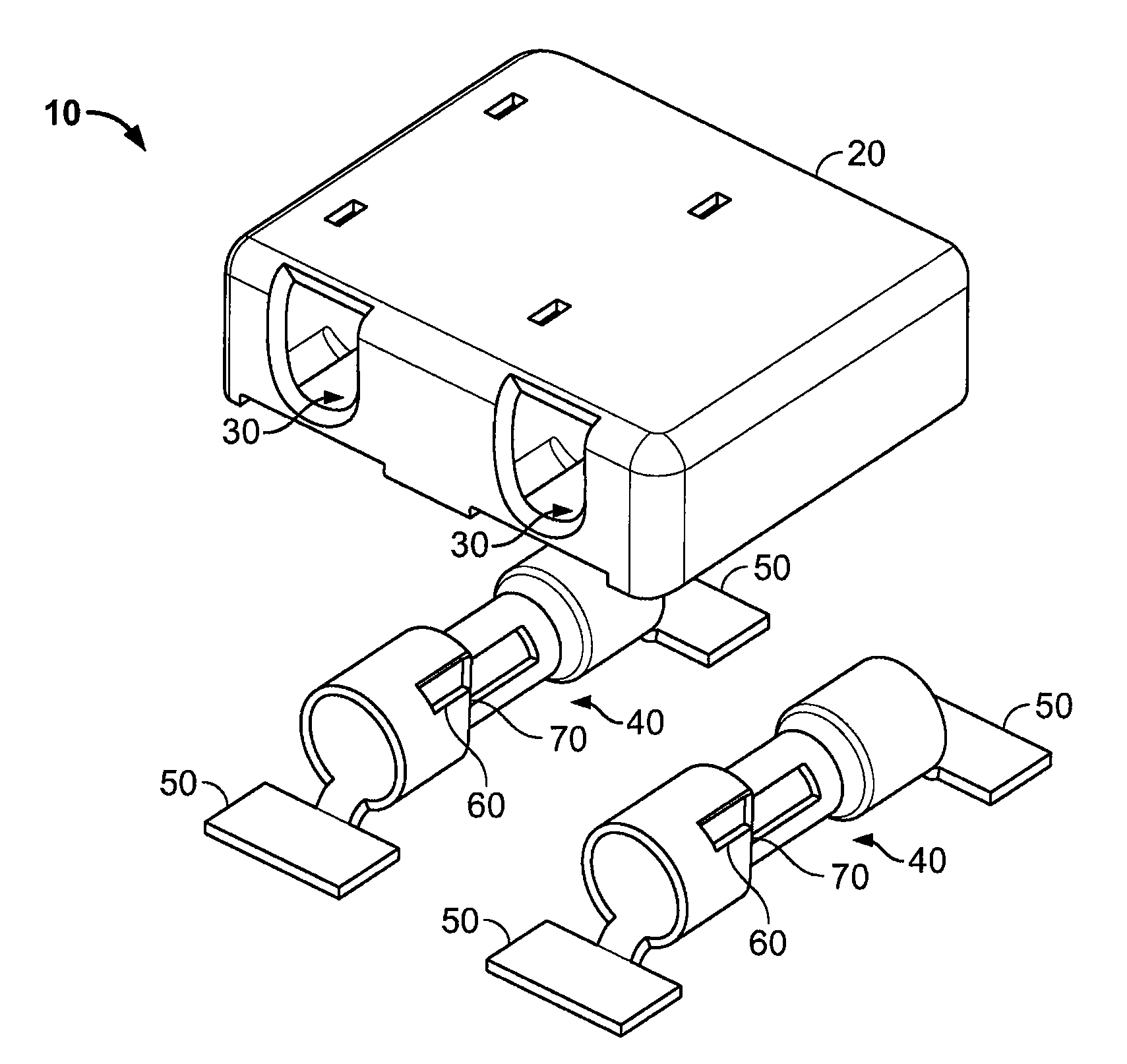
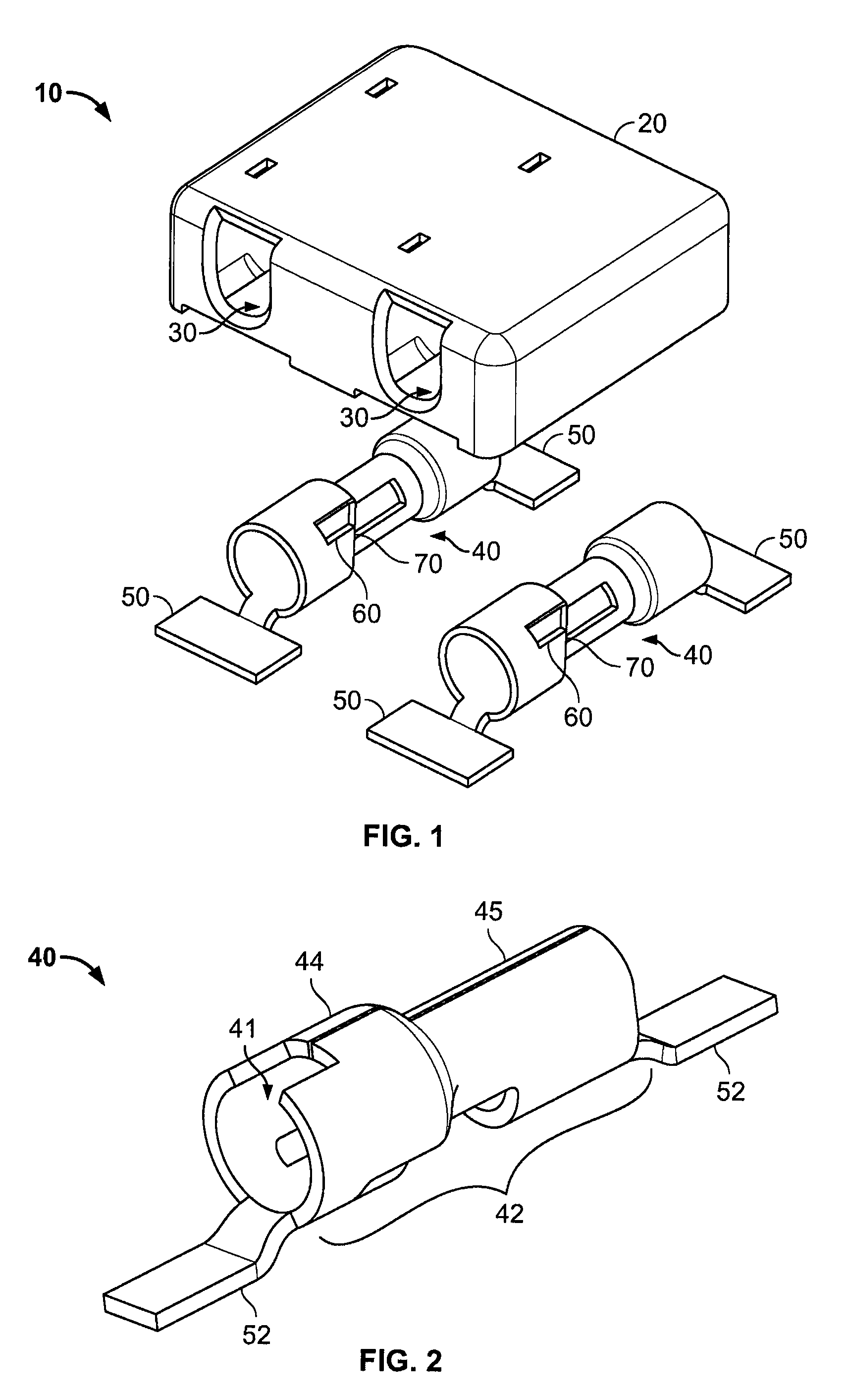
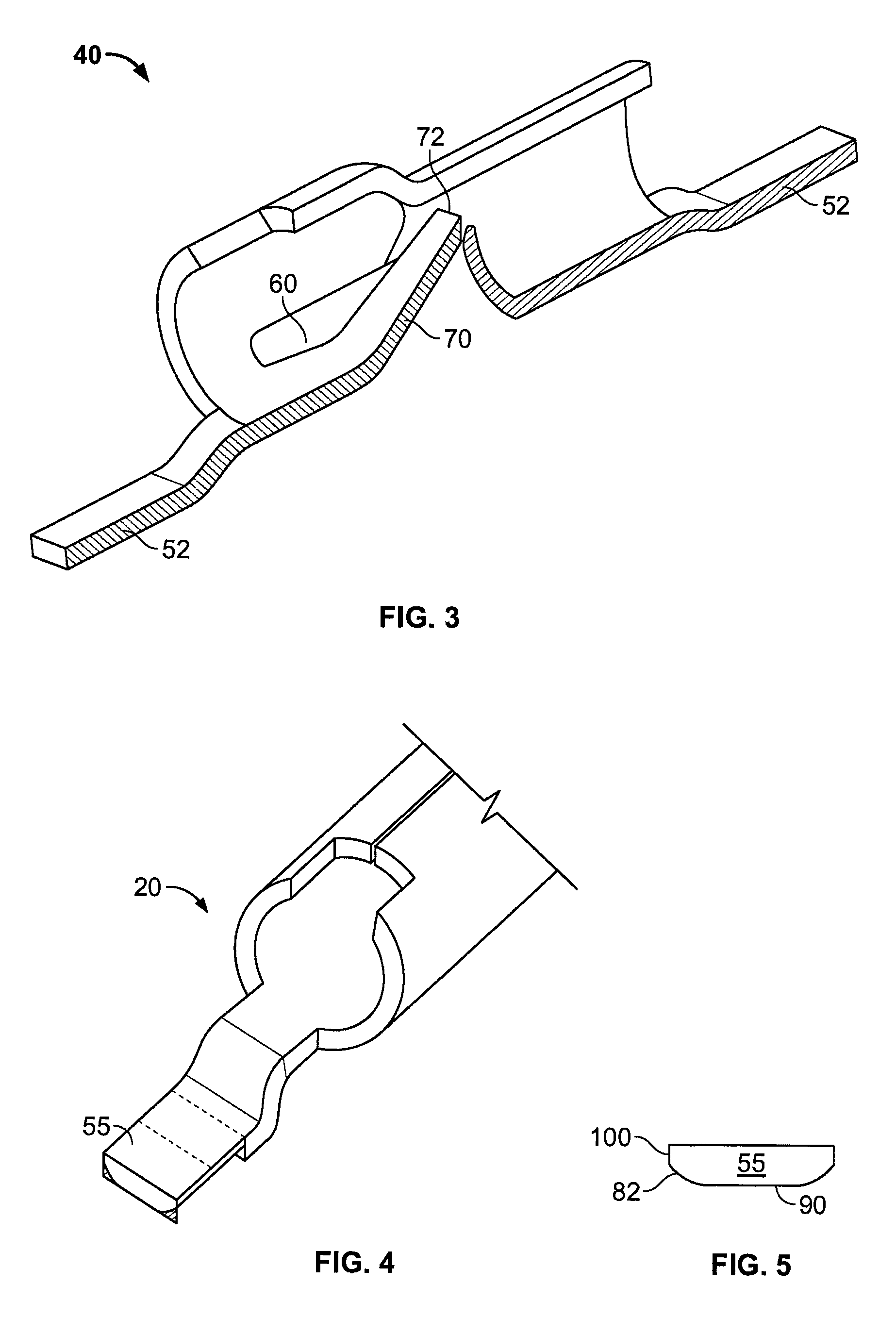
[0026]Referring to FIG. 1, an embodiment of the surface mounted electrical connector (SMEC) 10 is depicted. A SMEC 10 was formed of a housing 20 with at least one opening 30 and at least one contact 40. The housing 20 was formed of Zenite 6330®, a high temperature liquid crystalline polyester by E.I. du Pont de Nemours and Company of Wilmington, Del. The heat resistance of the housing allows it to be attached at the temperatures used to reflow solder the connector to the PCB surface.

[0027]The housing may ...


PUM


Abstract

A surface mount poke in connector is disclosed for mounting upon a surface of a printed circuit board, and is particularly applicable for printed circuit boards supporting LEDs. The connector has a securing means for engaging an inserted wire lead without the use of solder.

Description

CROSS-REFERENCE TO RELATED APPLICATIONS[0001]This application is related to co-pending application Ser. No. 11 / 063,065, filed Feb. 22, 2005 entitled “LOW PROFILE SURFACE MOUNT CONNECTOR” assigned to the assignee of the present invention and which is incorporated herein by reference in its entirety.FIELD OF THE INVENTION[0002]The present invention is directed to a low profile surface mount electrical connector (SMEC) for connecting wire leads to an electrical device constructed using surface mount technology (SMT). The electrical device may be a printed circuit board (PCB), but is not limited thereto. The PCB may contain light emitting diodes (LEDs). The invention is particularly well suited for connecting multiple PCBs in series.BACKGROUND OF THE INVENTION[0003]Electrical devices are often attached to printed circuit boards (PCBs) by soldering terminals of the electrical device to a surface of the PCB. Surface Mount Technology (SMT) is a particular method of soldering electrical ter...

Claims


Application Information

Patent Timeline
Patent Type & Authority Patents(United States)
IPC IPC(8): H01R11/20H01R12/55H01R12/57
CPCH01R4/4818H01R12/515H01R4/02H01R4/2404H01R12/57H01R13/03H01R13/422H01R43/0256H05K1/181H05K2201/10106H05K2201/10325H05K2201/10356H01R4/26Y02P70/50H01R4/48185H01R12/72H01R12/75
Inventor HORST, SHELDON LYNNDAILY, CHRISTOPHER G.
Owner TYCO ELECTRONICS LOGISTICS AG (CH)
Why Eureka
Try Eureka