Electrical process monitoring using mirror-mode electron microscopy

a technology of electron microscopy and electrical process monitoring, applied in the field of semiconductor manufacturing, can solve the problems of affecting the detection accuracy of electrical probes,

Active Publication Date: 2009-04-07
KLA TENCOR TECH CORP
View PDF18 Cites 96 Cited by
  • Summary
  • Abstract
  • Description
  • Claims
  • Application Information

AI Technical Summary

Benefits of technology

[0012]Another embodiment relates to an apparatus for inspecting a substrate using a projection electron beam system. The apparatus includes an illumination subsystem, an objective subsystem, a projection subsystem, a beam separator, and a control system. The beam separator is configured to receive the incident beam from the illumination subsystem, bend the incident electron beam towards t

Problems solved by technology

However, as device design rules further shrink, and new processes are being widely implemented, it becomes more challenging to detect defects in device structures with smaller design rules and higher aspect ratios.
Electrical probing disadvantageously requires special test structures to be included in the semiconductor dies being monitored.

Method used


Image

  • Electrical process monitoring using mirror-mode electron microscopy
  • Electrical process monitoring using mirror-mode electron microscopy
  • Electrical process monitoring using mirror-mode electron microscopy

Examples


Embodiment Construction

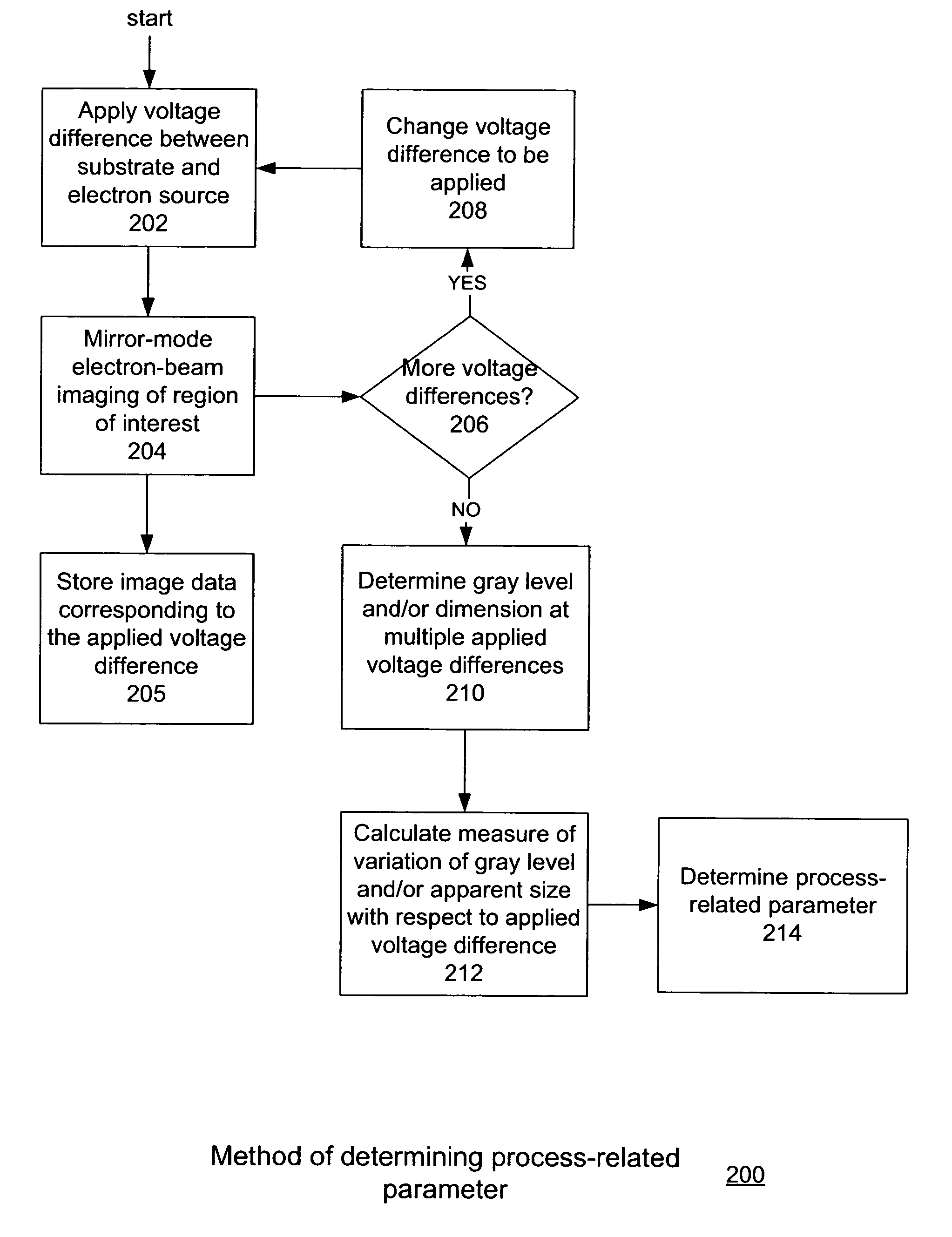
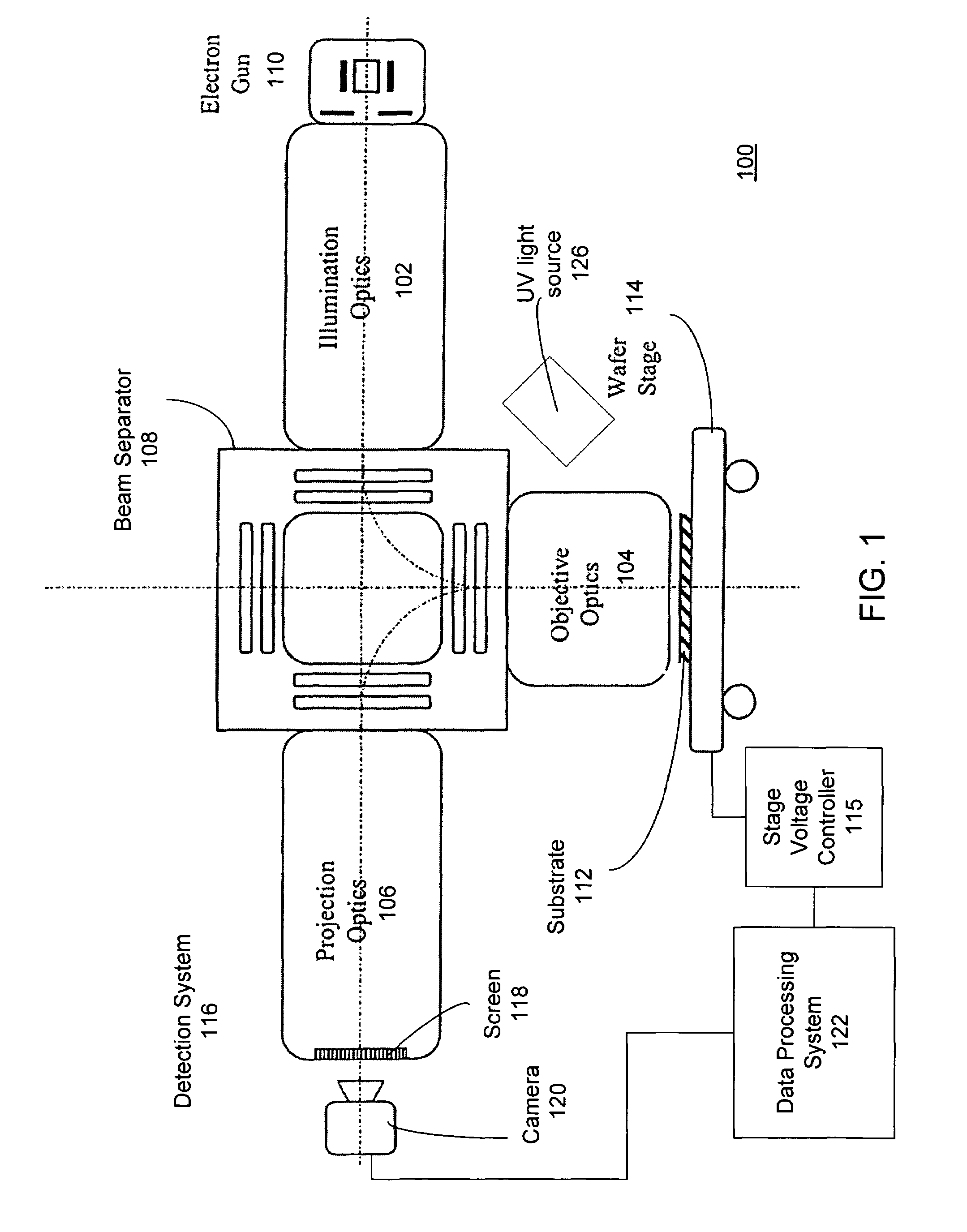
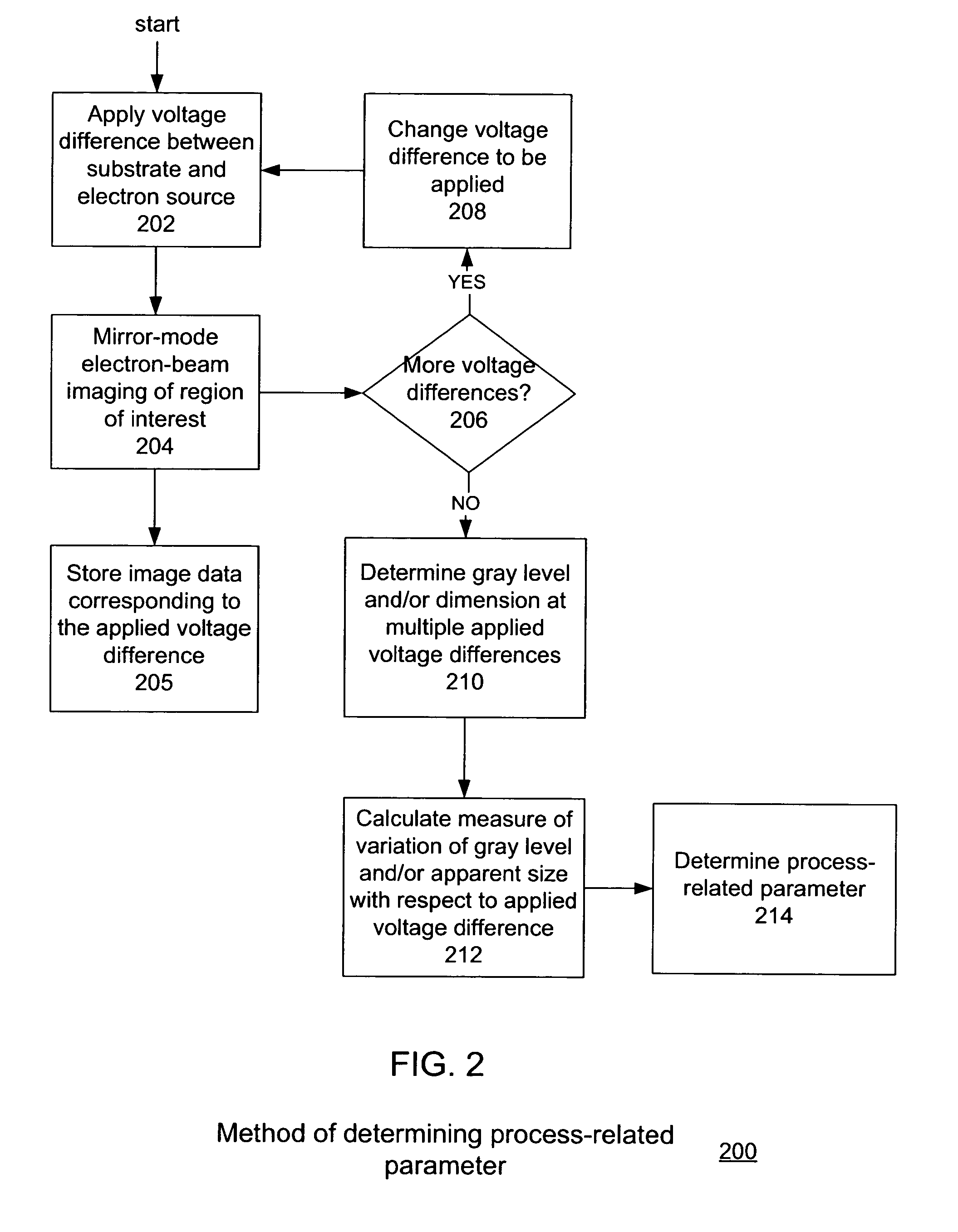
[0022]The technique disclosed herein and described below is advantageously capable of rapidly determining a process-related electrical parameter without the need for end-of-line probing or special test structures. Furthermore, this novel technique has been shown to have voltage contrast sensitivity in the tens of milli-volt range, which is orders of magnitude better than the sensitivity for typical scanning electron microscopes (SEMs). Typical SEMs have voltage contrast sensitivity of a few volts. Hence, the presently disclosed technique allows much more accurate measurements for electrical process monitoring, parametric measurement, and process control.

[0023]An alternative technique for determining a process-related parameter would be to incorporate an energy filter into a traditional SEM apparatus. However, energy filters with sub-volt resolution are complicated to design and manufacture, difficult to calibrate, and may have poor collection efficiency. The poor collection efficien...


PUM


Abstract

One embodiment relates to a method of inspecting a substrate using electrons. Mirror-mode electron-beam imaging is performed on a region of the substrate at multiple voltage differences between an electron source and a substrate, and image data is stored corresponding to the multiple voltage differences. A calculation is made of a measure of variation of an imaged aspect of a feature in the region with respect to the voltage difference between the electron source and the substrate. Other embodiments and features are also disclosed.

Description

BACKGROUND OF THE INVENTION[0001]1. Field of the Invention[0002]The present invention relates to semiconductor manufacturing. More particularly, the present invention relates to electrical process monitoring for semiconductor manufacturing.[0003]2. Description of the Background Art[0004]Automated inspection and review systems are important in process control and yield management for the semiconductor and related microelectronics industries. Such systems include optical and electron beam (e-beam) based systems.[0005]In the manufacture of semiconductor devices, detection of physical defects and electrical failure earlier in the fabrication process is becoming increasingly important to shorten product development cycles and increase product yield and productivity. Advanced wafer inspection systems based on scanning electron microscopy technology have been used to detect defects and electrical failure as voltage contrast defects. However, as device design rules further shrink, and new p...

Claims


Application Information

Patent Timeline
IPC IPC(8): H01L21/02G21K7/00H01J37/145
CPCH01J37/05H01J37/244H01J37/292H01J2237/24485H01J2237/24592H01J2237/2594H01J2237/2817
Inventor MARELLA, PAUL F.MCCORD, MARK A.MANKOS, MARIANADLER, DAVID L.
Owner KLA TENCOR TECH CORP
Why Eureka
Try Eureka