Method for generating minimal leakage current input vector using heuristics
a leakage current input and input vector technology, applied in the field of integrated circuits, can solve the problems of severe power problem of devices, manual determination of predetermined input vectors, etc., and achieve the effect of reducing the leakage curren
- Summary
- Abstract
- Description
- Claims
- Application Information
AI Technical Summary
Benefits of technology
Problems solved by technology
Method used
Image
Examples
Embodiment Construction
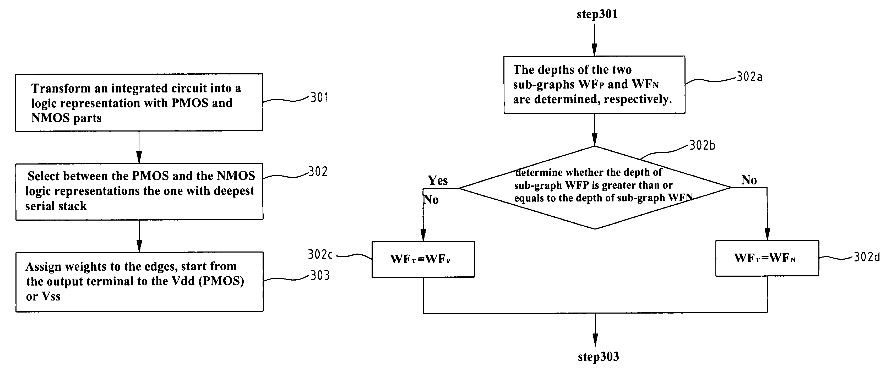
[0018]FIG. 3A shows a flowchart illustrating the method for generating input vector for minimizing the leakage current of the present invention. Referring to FIG. 3A, step 301 is to transform an integrated circuit, for example a CMOS circuit, into a logic representation with PMOS and NMOS parts. To more understand the operation of step 301, consider the following detailed description. For a given CMOS circuit, Vdd, Vss, output terminals and all wire connection points are transformed into nodes, and P and N devices of the given CMOS circuit are transformed into edges. To simplify the graph, only one node is used to represent connected edges. For example, if there are 10 devices directly connected to an output terminal, only one node is used to represent the output terminal. The transformed weighted graph is called WF, including two sub-graphs called, WFP (for PMOS) and WFN (for NMOS), respectively.
[0019]Step 302 in FIG. 3A is to select between the PMOS and the NMOS logic representati...
PUM
 Abstract
Description
Claims
Application Information


