Pixel structure and active matrix substrate

a technology of active matrix and pixel structure, applied in the field of pixel structure and active matrix substrate, can solve the problems of serious image sticking phenomenon and color washout phenomenon, and achieve the effect of effectively reducing the accumulation of charge in the pixel structur

Active Publication Date: 2009-04-14
AU OPTRONICS CORP
View PDF3 Cites 13 Cited by
  • Summary
  • Abstract
  • Description
  • Claims
  • Application Information

AI Technical Summary

Benefits of technology

[0010]The present invention is directed to provide a pixel structure to effectively avoid image sticking phenomenon.
[0011]The present invention is directed to provide an active matrix substrate to effectively avoid image sticking phenomenon.
[0019]Since the charge releasing device (capacitor or TFT) is used in the present invention, the charge accumulation in the pixel structure can be effectively reduced while pixel structure is driven.

Problems solved by technology

In other words, when a viewer sees from a different angle, the brightness (gray level) displayed by the conventional MVA TFT-LCD panel 100 varies, which results in color washout phenomenon.
Thus, the voltage level of the floating pixel electrode 214 is accordingly shifted, which causes a serious image sticking phenomenon in the above-described wide viewing technologies.

Method used


Image

  • Pixel structure and active matrix substrate
  • Pixel structure and active matrix substrate
  • Pixel structure and active matrix substrate

Examples


first embodiment

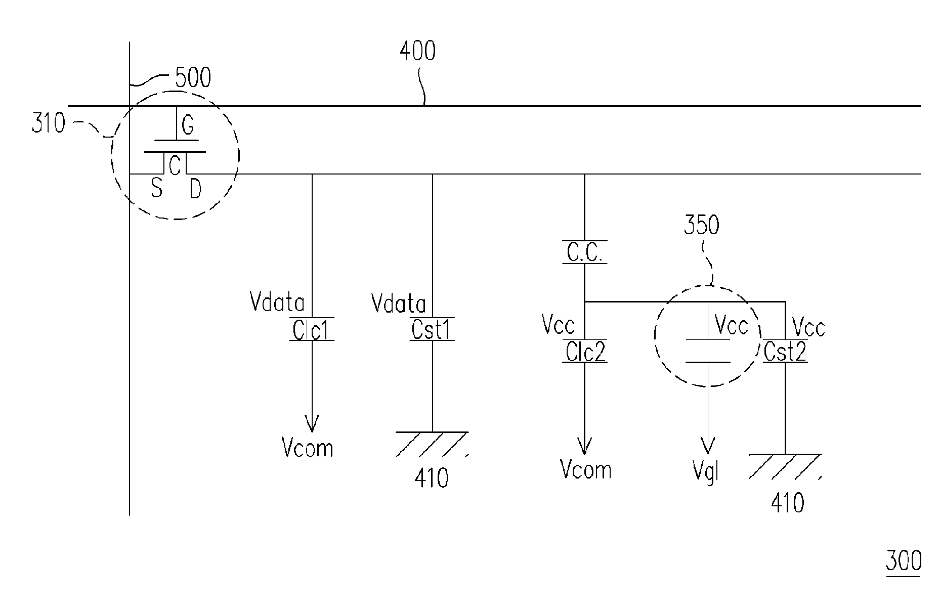
[0031]FIG. 3 is a top view of a pixel structure according to the first embodiment of the present invention. Referring to FIG. 3, the pixel structure 300 of the embodiment is electrically connected to a scan line 400 and a data line 500. The pixel structure 300, as shown in FIG. 3, includes an active device 310, a first pixel electrode 320, a second pixel electrode 330, a capacitor coupling electrode 340 and a charge releasing device 350. The active device 310 is electrically connected to the scan line 400 and the data line 500. The first pixel electrode 320 is electrically connected to the data line 500 through the active device 310. The second pixel electrode 330 is electrically isolated from the first pixel electrode 320. The capacitor coupling electrode 340 is disposed under the second pixel electrode 330, and electrically connected to the data line 500 through the active device 310. The charge releasing device 350 is electrically connected to the second pixel electrode 330.

[0032...

second embodiment

[0043]FIG. 6 is a top view of a pixel structure according to the second embodiment of the present invention. The pixel structure 300′ of the embodiment is similar to the pixel structure 300 in the first embodiment except that the pixel structure 300′ is electrically controlled by a first TFT 310a (thin film transistor) and a second TFT 310b. The first TFT 310a is electrically connected to a first pixel electrode 320 while the second TFT 310b is electrically connected to a second pixel electrode 330. The ratio of the width over length (W / L) of the second TFT 310b is substantially smaller than the (W / L) of the first TFT 310a.

[0044]The first TFT 310a in the second embodiment has, for example, a first gate electrode G1, a first channel layer C1, a first source electrode S1 and a first drain electrode D1. The first gate electrode G1 is electrically connected to or integrated with the scan line 400. The first source electrode S1 is electrically connected to or integrated with the data li...


PUM

PropertyMeasurementUnit
voltageaaaaaaaaaa
electricallyaaaaaaaaaa
voltageaaaaaaaaaa

Abstract

A pixel structure electrically connected to a scan line and a data line, includes an active device, a first pixel electrode, a second pixel electrode, a capacitor coupling electrode and a charge releasing device. The active device is electrically connected to the scan line and the data line. The second pixel electrode is electrically isolated from the first pixel electrode. The capacitor coupling electrode is disposed under the second pixel electrode and electrically connected to the data line through the active device. The charge releasing device is electrically connected to the second pixel electrode. The above-described pixel structure is able to effectively solve the image sticking problem. In addition, further provides an active matrix substrate which is able to avoid the image sticking effect.

Description

CROSS-REFERENCE TO RELATED APPLICATION[0001]This application claims the priority benefit of Taiwan application serial no. 94116051, filed on May 18, 2005. All disclosure of the Taiwan application is incorporated herein by reference.BACKGROUND OF THE INVENTION[0002]1. Field of Invention[0003]The present invention relates to a pixel structure and an active matrix substrate and, more particularly, to a pixel structure and an active matrix substrate capable of avoiding image sticking phenomenon.[0004]2. Description of the Related Art[0005]Nowadays, it is the trend that a TFT-LCD (thin film transistor liquid crystal display) should have the characteristics such as high contrast ratio, no gray scale inversion, little color shift, high luminance, high color richness, high color saturation, fast response and wide viewing angle. Among the wide viewing technologies, there are a few types of LCDs, such as TN+FILM (twisted nematic LCD plus wide viewing film), IPS-LCD (in-plane switching LCD), F...

Claims


Application Information

Patent Timeline
Patent Type & Authority Patents(United States)
IPC IPC(8): G02F1/1343
CPCG02F1/136213G02F1/133707G02F1/134309H01L27/13
Inventor CHEN, YI-JENTSAO, CHENG-HANHUANG, WEI-KAIWU, MING-CHOUTSAI, CHEN-SHUNWANG, CHIUNG-PINHUANG, YI-PAI
Owner AU OPTRONICS CORP
Why Eureka
Try Eureka