Method of manufacturing a semiconductor device

a manufacturing method and semiconductor technology, applied in the direction of printed circuit manufacturing, printed circuit assembling, basic electric elements, etc., can solve the problems of mechanical warping, waste of resin, and hampering efforts to make the outer dimensions of molding resin smaller and thinner

Active Publication Date: 2009-04-21
TEXAS INSTR INC
View PDF2 Cites 35 Cited by
  • Summary
  • Abstract
  • Description
  • Claims
  • Application Information

AI Technical Summary

Benefits of technology

[0016]For the manufacturing method, it is preferred that there also be a process step in which the atmosphere around the liquid resin is evacuated before molding the liquid resin by means of the recesses of the mold part. Because the atmosphere of the semiconductor element is evacuated, it is possible to inhibit gas bubbles and voids in the molding resin. The degree of absolute vacuum is 5 kPa or better.

Problems solved by technology

However, the aforementioned molding methods of the prior art have the following problems.
In addition, when the plural semiconductor chips are molded as a block, it is necessary to feed unnecessary resin between adjacent semiconductor chips, so that wasted resin results.
This hampers efforts to make the outer dimensions of the molding resin smaller and thinner.
As a result, the difference in thermal expansion coefficients of the principal materials used in the package cause mechanical warping.
This warping prevents the terminals of the package (solder balls) from making contact with the terminals on the mother substrate, leading to contact defects.
Because the gate is cut mechanically, the outer dimensional accuracy and the appearance of the package may become defective.
In addition, residual resin is created after resin sealing, and this leads to poor assembly when the IC package is stacked.

Method used


Image

  • Method of manufacturing a semiconductor device
  • Method of manufacturing a semiconductor device
  • Method of manufacturing a semiconductor device

Examples


first embodiment

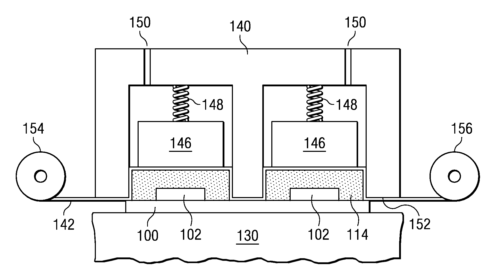
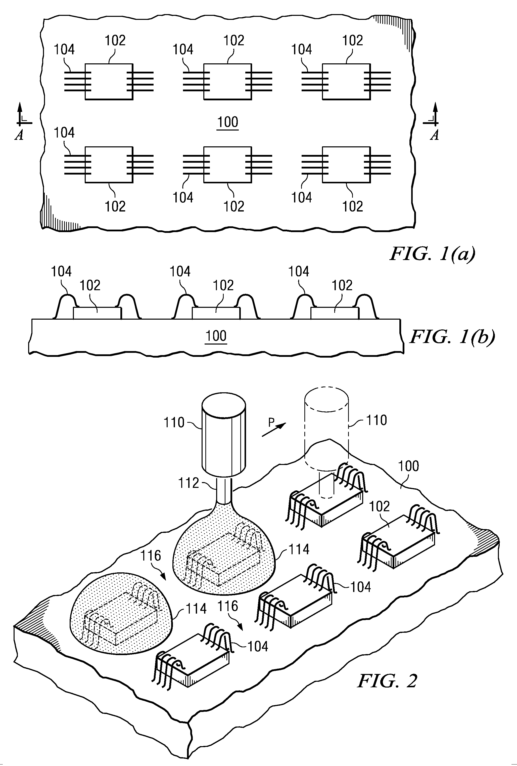
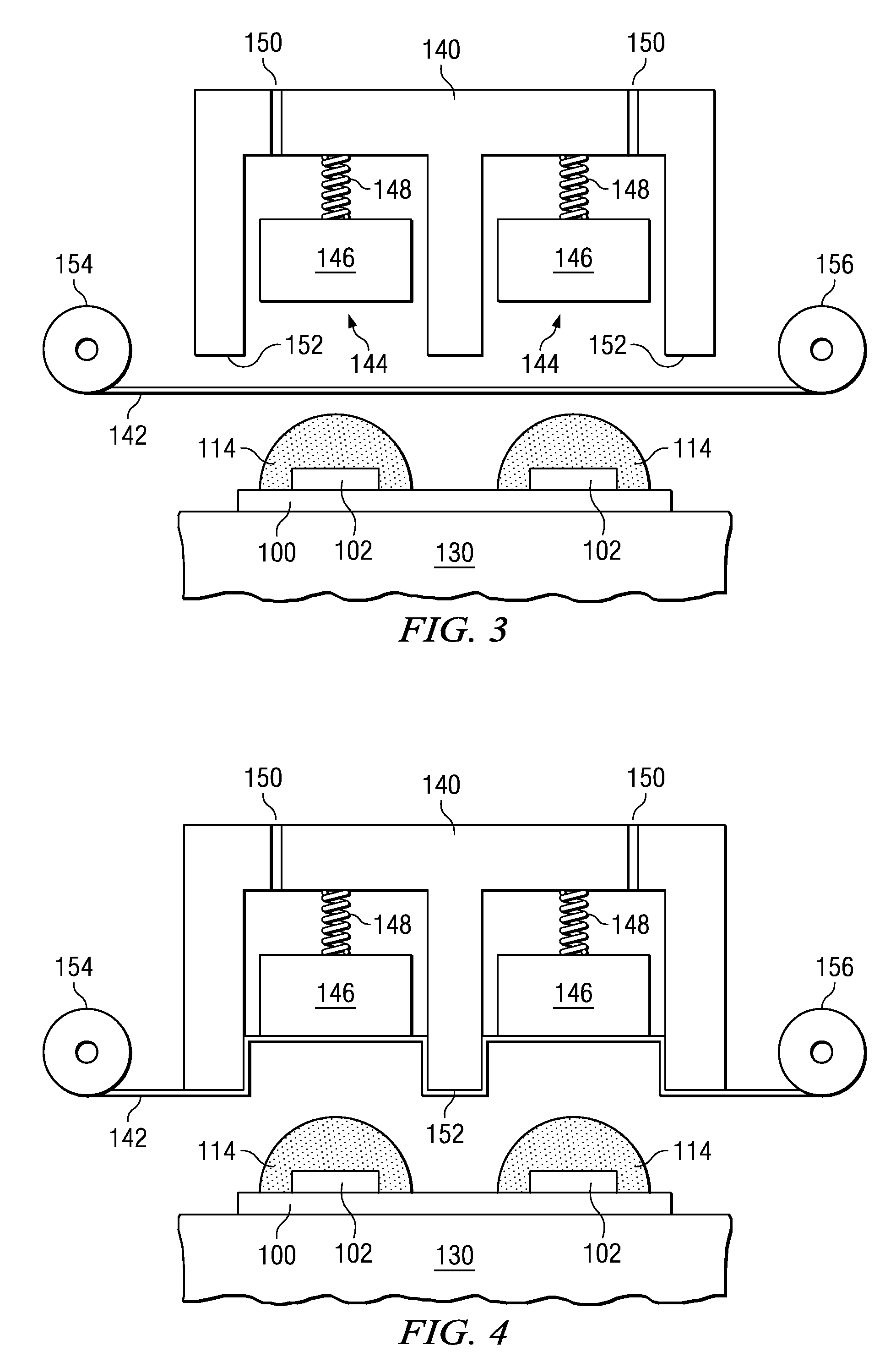
[0037]FIG. 1(a) is a plan view illustrating a substrate with plural semiconductor chips mounted on it, and FIG. 1(b) is a cross section taken across A-A. In the first embodiment, plural semiconductor chips are set in matrix configuration on one surface of substrate 100. There is no special limitation on the constitution of said substrate 100. It is possible to adopt multilayer wiring substrates and film substrates. For example, a glass epoxy resin, polyimide resin, or other insulating substrate can be used. Said semiconductor chips 102 are attached via die attachment or the like at the prescribed positions of substrate 100. The electrodes of semiconductor chips 102 are connected to the copper pattern formed on the surface of substrate 100 by means of bonding wires 104.

[0038]In the following, the method will be explained for individually molding said semiconductor chips 102 mounted on the substrate shown in FIG. 1 as a block. As shown in FIG. 2, container 110 filled with liquid resin...

embodiment 2

[0052]FIG. 9 is a plan view illustrating the state in which the semiconductor element has been molded using the upper die in To simplify the explanation, only a single region of the substrate is shown here. On the upper surface of substrate 100, plural lands 182 are formed connected to a copper pattern. Said lands 182 are regions connected to the solder balls on the inner surface of the substrate via the through-holes formed in substrate 100. The various semiconductor elements on substrate 100 are sealed by molding resin 184. Said molding resin 184 has chamfers 186 formed at the corners matching cavity 144 in upper die 140. In addition, fine protrusions 188 corresponding to air pockets 180 are formed on chamfers 186 of molding resin 184.

[0053]In this embodiment, it is possible to eliminate the generation of voids in molding resin 184 by providing air pockets 180. Consequently, it is possible to increase the package yield. The size of air pocket 180 should be appropriate to provide ...


PUM

PropertyMeasurementUnit
glass transition temperatureaaaaaaaaaa
viscosityaaaaaaaaaa
thickaaaaaaaaaa

Abstract

The objective of the invention is to provide a method of manufacturing a semiconductor device that allows individual molding of plural semiconductor chips carried on a surface of the substrate. It includes the following process steps: a process step in which plural semiconductor elements 102 are arranged on the surface of substrate 100; a process step in which the inner side of substrate 102 is fixed on lower die 130; a process step in which liquid resin 114 is supplied from nozzle 112 onto each of the semiconductor elements in order to cover at least a portion of each of semiconductor chips 102; a process step in which the upper die having plural cavities 144 formed in one surface is pressed onto the lower die, and liquid resin 114 is molded at a prescribed temperature by means of plural cavities 144; and a process step in which cavities 144 of upper die 140 are detached from the substrate, and plural molding resin portions are formed individually.

Description

FIELD OF THE INVENTION[0001]The present invention is concerned with the methods for sealing plural semiconductor chips mounted on one surface of a substrate, especially a molding method which can be adapted for the development of small, thin semiconductor devices.[0002]The popularity of cell phones, portable computers, and other small electronic equipment, has created ever-increasing demand for the development of small, thin semiconductor devices installed in them. In order to meet this demand, researchers have developed BGA and CSP packages, which have been adopted in practical applications.[0003]Patent Reference 1 discloses a type of BGA package. As shown in FIG. 13, plural copper pattern portions 4 are formed on the surface of insulating film substrate 3 made of polyimide for electric connection between semiconductor chip 2 and solder bumps 7. One end of each said copper pattern portion 4 is connected via through-hole 3a formed in insulating film substrate 3 to solder bump 7. The...

Claims


Application Information

Patent Timeline
Patent Type & Authority Patents(United States)
IPC IPC(8): H05K3/30
CPCH01L21/561H01L21/566H01L21/67126H01L23/3107H01L23/3128H01L24/97H01L25/105H01L2224/48091H01L2224/4824H01L2224/97H01L2924/01015H01L2924/01029H01L2924/01082H01L2924/14H01L2924/15311H01L2924/15331H01L2924/3511H01L24/48H01L2924/01005H01L2924/01006H01L2924/01033H01L2924/014H01L2225/1023H01L2225/1058H01L2224/32225H01L2224/48227H01L2224/48465H01L2224/73265H01L2224/49175H01L2224/32245H01L2224/48247H01L2224/73215H01L2224/32013H01L2924/10253Y10T29/4913Y10T29/49146H01L2224/85H01L2924/00014H01L2924/00H01L2924/00012H01L24/49H01L24/73H01L2924/181H01L2224/45099H01L2224/45015H01L2924/207
Inventor TAKAHASHI, YOSHIMIAMAGAI, MASAZUMI
Owner TEXAS INSTR INC
Why Eureka
Try Eureka