Clock enable throttling for power savings in a memory subsystem

a technology of memory subsystem and clock, which is applied in the direction of liquid/fluent solid measurement, sustainable buildings, instruments, etc., can solve the problems of increasing the electrical load of parallel data and address buses, increasing the power consumption of memory systems, and increasing the electrical load of memory systems

Active Publication Date: 2009-04-21
ORACLE INT CORP
View PDF22 Cites 31 Cited by
  • Summary
  • Abstract
  • Description
  • Claims
  • Application Information

AI Technical Summary

Benefits of technology

[0006]Various embodiments of a system and methods of throttling a clock of a memory subsystem are disclosed. In one embodiment, a memory subsystem comprises a memory controller coupled to one or more memory modules. Each memory module comprises a buffer coupled to one or more memory ranks. A clock source is coupled to provide a clock signal to each of the memory modules. The memory controller is configured to convey a first clock enable (CKE) command to at least one of the memory modules, the CKE command corresponding to a given memory rank. In response to the first CKE command, a memory module buffer associated with the given memory rank is configured to convey a CKE disable signal to the given memory rank. The given memory rank is configured to disable operation of the clock signal within at least a portion of the given memory rank, responsive to the CKE disable signal.

Problems solved by technology

Consequently, computer memory systems have seen an increase in power consumption.
A parallel architecture suffers from the problem that each additional memory module increases the electrical loading on the parallel data and address buses.
However, the resulting increase in the number of modules that the system can support increases the power consumption of the memory system.
The speed of memory modules, rather than the speed of processors, is often the limiting factor for memory transactions.
Unfortunately, power dissipation is directly proportional to clock speed for a typical memory module.

Method used


Image

  • Clock enable throttling for power savings in a memory subsystem
  • Clock enable throttling for power savings in a memory subsystem
  • Clock enable throttling for power savings in a memory subsystem

Examples


Embodiment Construction

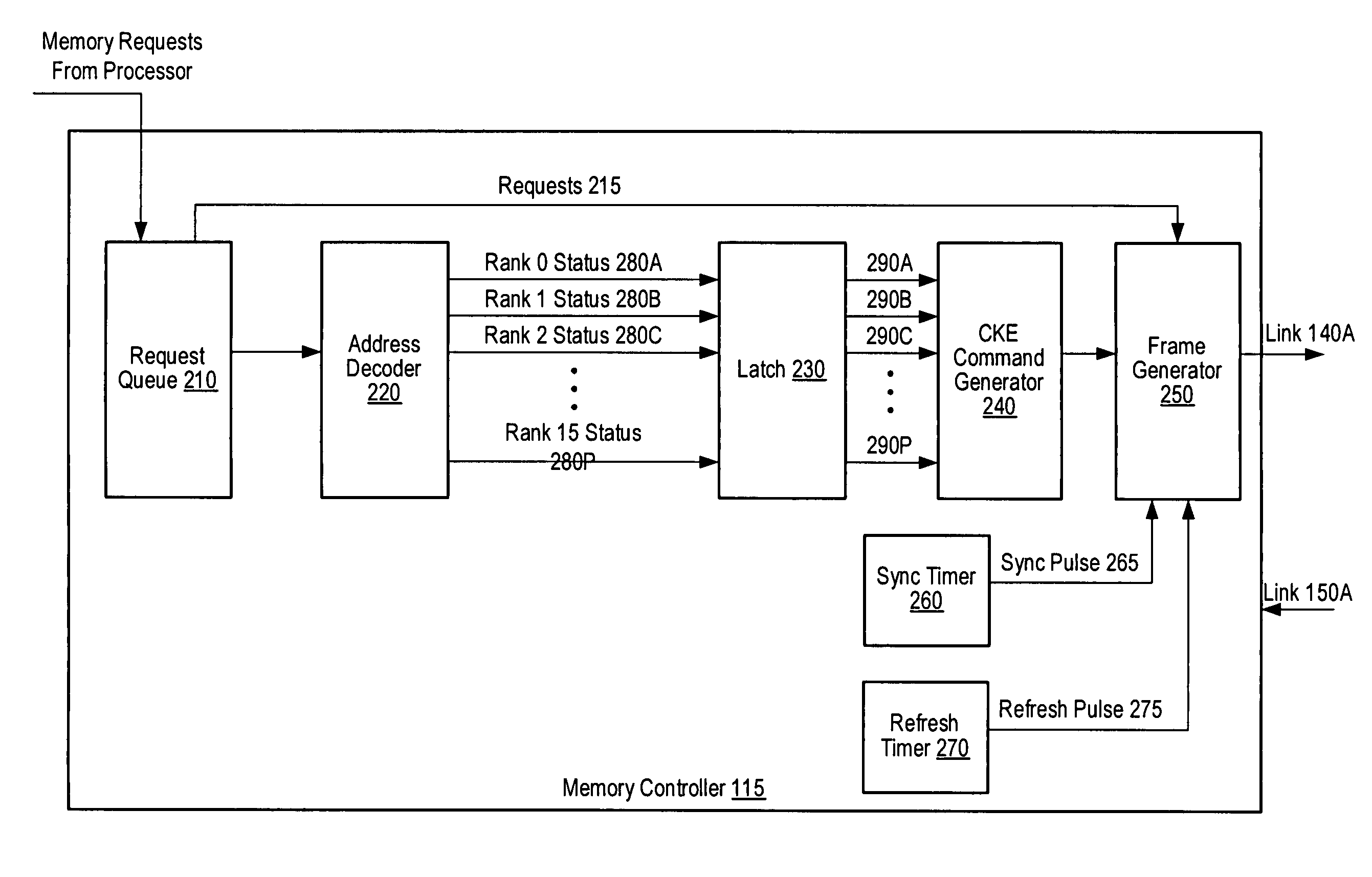
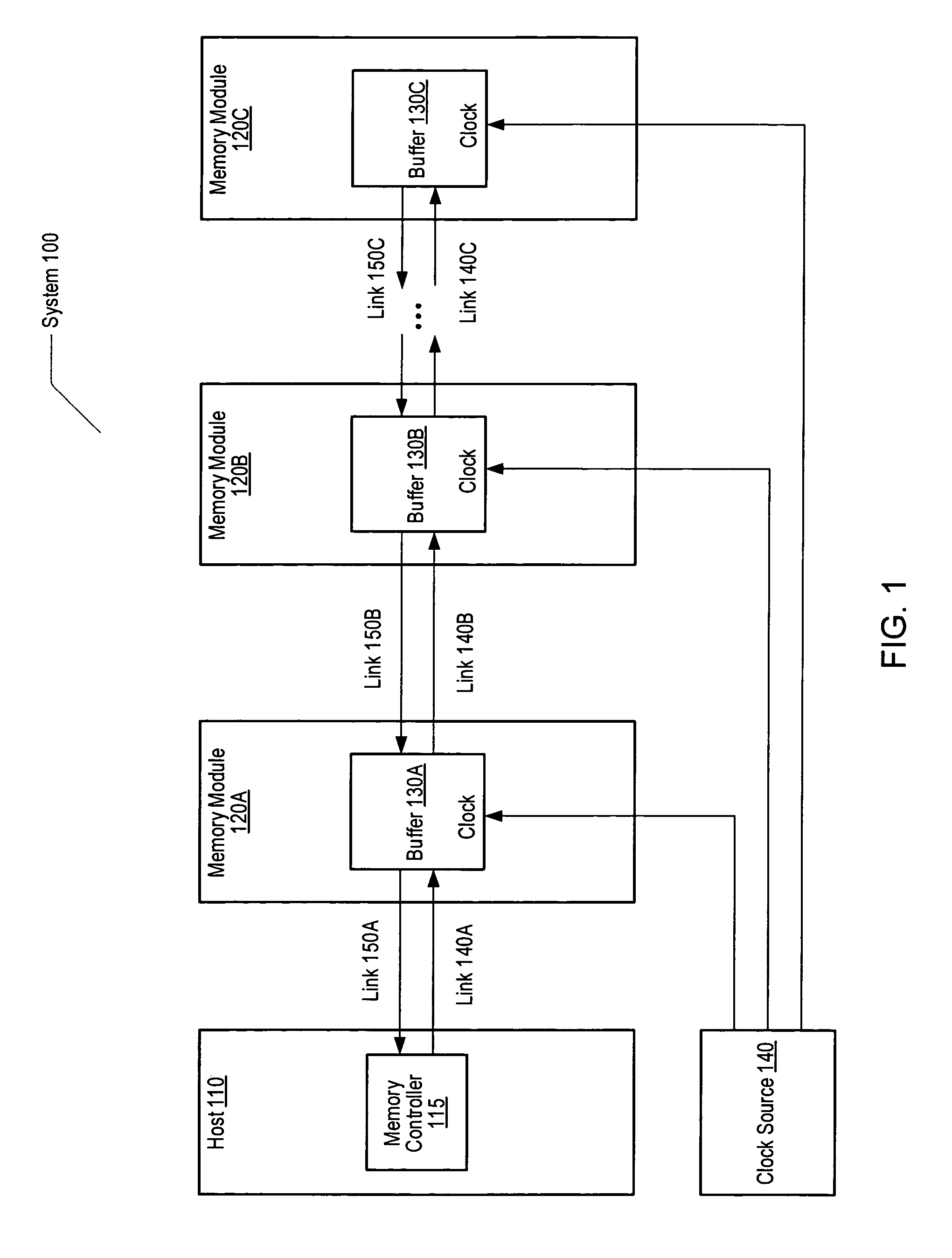
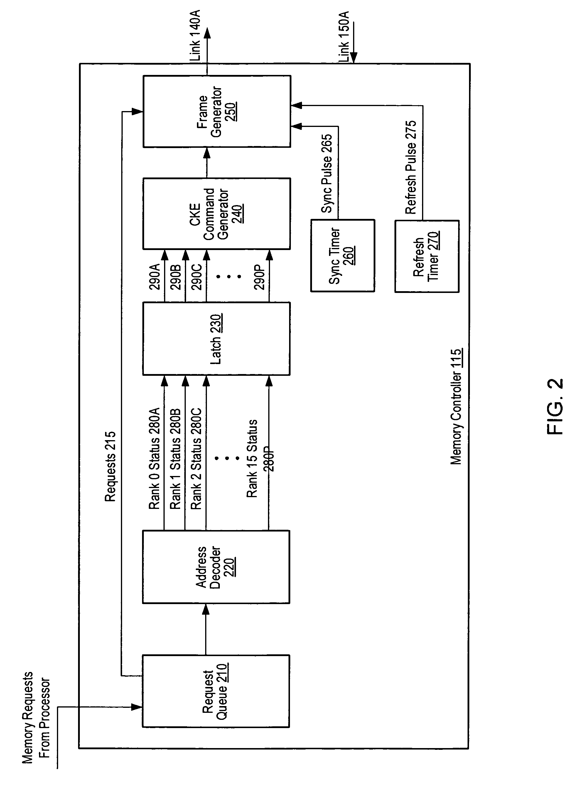
[0021]FIG. 1 is a generalized block diagram of one embodiment of a computer memory system 100 including a host 110, one or more memory modules 120A-120C, and a clock source 140. In the discussions that follow, elements designated by a number followed by a letter may be referred to collectively using the number alone. For example, memory modules 120A-120C may be referred to collectively as memory modules 120. In the illustrated embodiment, host 110 may be a processor that includes a memory controller 115. In an alternative embodiment, a processor and a memory controller may be separate elements of host 110.

[0022]In one embodiment, each of memory modules 120 may be a fully buffered dual inline memory module (FB-DIMM) that includes a respective buffer 130A-130C. Buffers 130 may provide an interface between an array of DRAM devices and other FB-DIMMs or host 110 within system 100. The JEDEC Solid State Technology Association has published a draft specification for FB-DIMMs. The JEDEC FB...


PUM


Abstract

A memory subsystem is disclosed. The memory subsystem includes a memory controller coupled to one or more memory modules. Each memory module comprises a buffer coupled to one or more memory ranks. A clock source is coupled to provide a clock signal to each of the memory modules. The memory controller is configured to convey a clock enable (CKE) command to one of the memory modules, the CKE command corresponding to a given memory rank. In response to the CKE command, a memory module buffer associated with the given memory rank is configured to convey a CKE disable signal to the given memory rank. The given memory rank is configured to disable operation of the clock signal within the given memory rank, responsive to the CKE disable signal.

Description

BACKGROUND OF THE INVENTION[0001]1. Field of the Invention[0002]This invention relates to computer memory systems and, more particularly, to techniques for reducing power consumption of computer memory systems.[0003]2. Description of the Related Art[0004]Evolving standards for computer memory systems have lead to systems that include greater numbers of higher capacity memory devices. Consequently, computer memory systems have seen an increase in power consumption. One technology in particular, the Fully Buffered Dual Inline Memory Module (FBDIMM), achieves very high memory density by allowing memory modules to be connected in series, rather than in parallel. A parallel architecture suffers from the problem that each additional memory module increases the electrical loading on the parallel data and address buses. The serial point-to-point architecture used by FB-DIMMs overcomes the electrical loading problem since electrical loading is not changed when another module is added. Howeve...

Claims


Application Information

Patent Timeline
Patent Type & Authority Patents(United States)
IPC IPC(8): G06F13/00G06F1/26G11C8/18
CPCG06F1/3225G06F1/3237G06F1/3275G06F13/4243G11C5/04G11C8/06G11C8/18G11C5/144Y02B60/1228Y02B60/1221Y02B60/1235Y02D10/00
Inventor KAPIL, SANJIVWYNN, AARON S.
Owner ORACLE INT CORP
Why Eureka
Try Eureka