
Semiconductor device and method for manufacturing the same

a technology of semiconductor devices and semiconductors, applied in semiconductor devices, semiconductor/solid-state device details, electrical apparatus, etc., can solve problems such as poor step coverage, voids may become serious problems, and discontinuous deposition points, so as to prevent overhangs or voids

Inactive Publication Date: 2009-04-28
DONGBU ELECTRONICS CO LTD
View PDF8 Cites 0 Cited by
  • Summary
  • Abstract
  • Description
  • Claims
  • Application Information

AI Technical Summary

Benefits of technology

"The present invention provides a semiconductor device and a method for manufacturing the same that can prevent overhang or voids during the process of forming a diffusion barrier layer and a seed layer. This prevents degradation of the performance and reliability of the semiconductor device. The semiconductor device includes a semiconductor substrate, an interlayer dielectric layer, a diffusion barrier layer, and a seed layer. The method includes forming an interlayer dielectric layer, a first photoresist layer, a shielding layer, a second photoresist layer, etching the shielding layer, developing and removing a portion of the first photoresist layer, and forming a hole by etching the interlayer dielectric layer."

Problems solved by technology

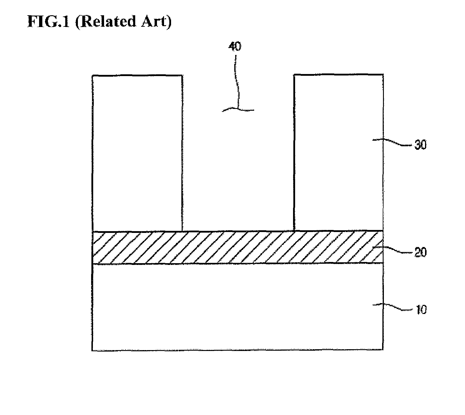
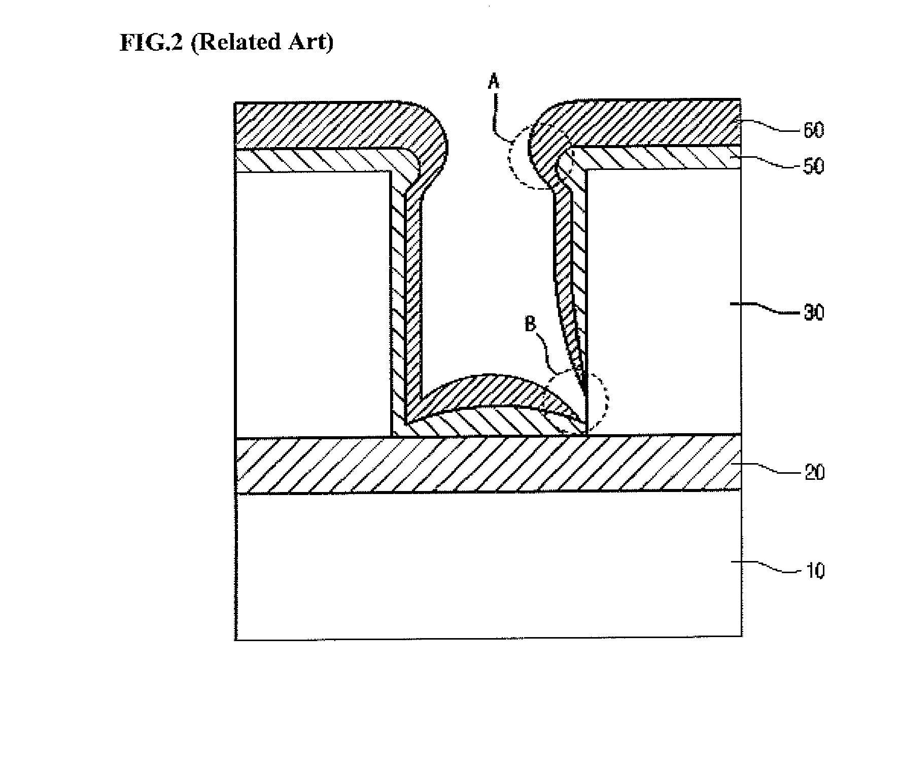
However, a reduction of the via size and an increase of the step difference may cause a poor step coverage, so that overhang A or a deposition discontinuous point B may occur.
Further, according to the related art, such overhang, deposition discontinuous point and voids may become serious problems because the aspect ratio of the hole may increase as the degree of integration of the semiconductor device increases.

Method used


Image

  • Semiconductor device and method for manufacturing the same
  • Semiconductor device and method for manufacturing the same
  • Semiconductor device and method for manufacturing the same

Examples


Embodiment Construction

[0016]Hereinafter, a semiconductor device and a method for manufacturing the same according to an exemplary embodiment of the present invention will be explained in detail with reference to accompanying drawings.

[0017]In the following description, the expression “formed on each layer” may include the meaning of both “formed directly on each layer” and “formed indirectly on each layer”.

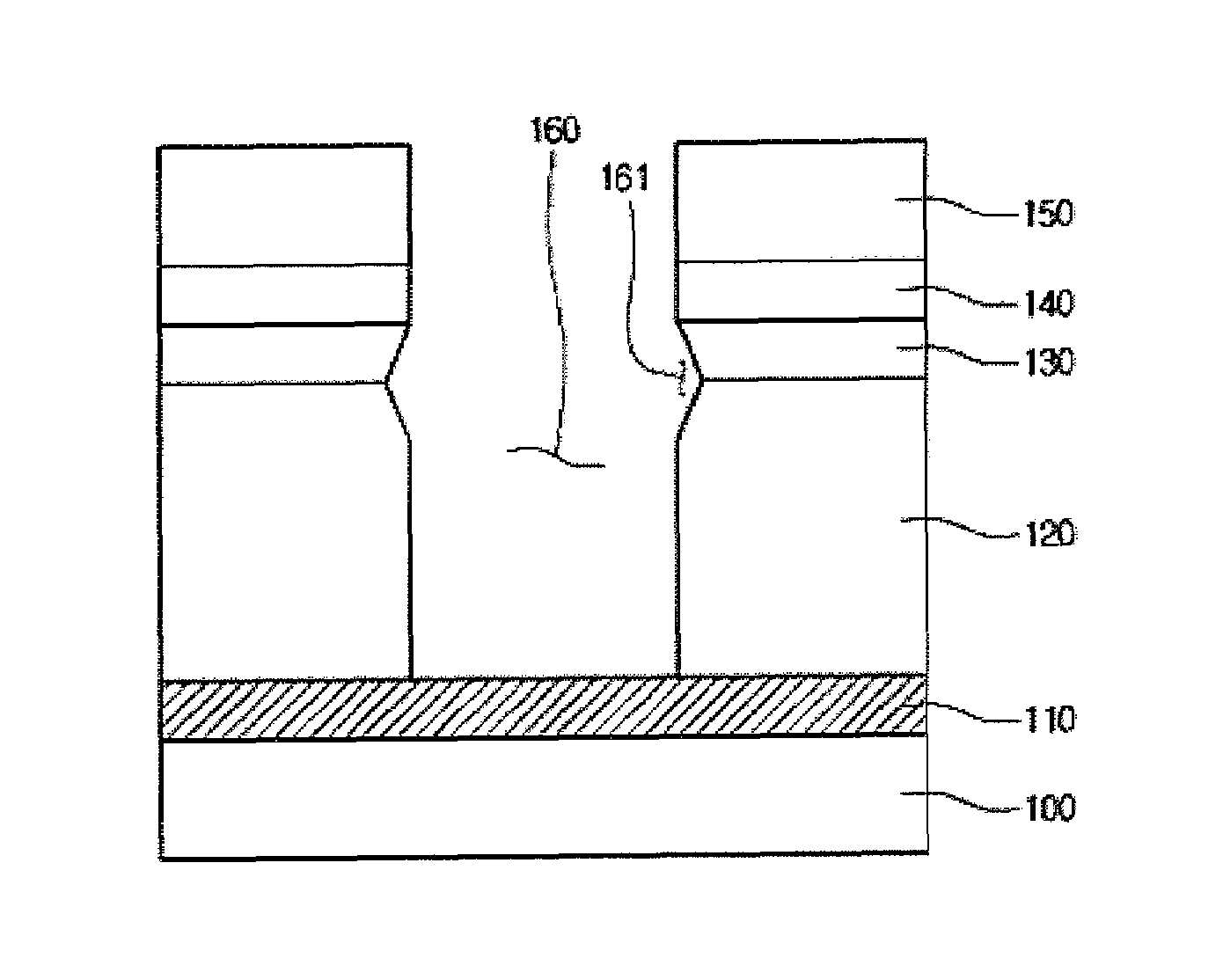
[0018]FIGS. 4 to 12 illustrate a method for forming a metal interconnection of a semiconductor device in accordance with an exemplary embodiment of the present invention.

[0019]Referring to FIG. 4, an interlayer dielectric layer 120 is formed on a semiconductor substrate 100 where a conductive layer 110 is formed.

[0020]Then, referring to FIG. 5, a photoresist is coated on the interlayer dielectric layer 120 to a predetermined thickness so as to form a first photoresist layer 130. The first photoresist layer 130 can have a thickness such that the width of the undercut portion can be controlled.

[0021]In a...


PUM


Abstract

A semiconductor device and a method for manufacturing the same is provided. The semiconductor device includes a semiconductor substrate having a conductive layer; an interlayer dielectric layer formed on the semiconductor substrate, the interlayer dielectric layer having a hole with a taper angled at the hole's upper portion; a diffusion barrier layer formed on the hole and the interlayer dielectric layer; and a seed layer formed on the diffusion barrier layer.

Description

RELATED APPLICATION(S)[0001]This application claims the benefit under 35 USC §119(e) of Korean Patent Application No. 10-2005-0129865 filed Dec. 26, 2005, which is incorporated herein by reference in its entirety.FIELD OF INVENTION[0002]The present invention relates to a semiconductor device and a method for manufacturing the same.BACKGROUND OF THE INVENTION[0003]In general, there has been a rapid change toward high performance in next generation semiconductor devices. As a result, a via hole size has become reduced and the aspect ratio thereof has become increased. Thus, superior step coverage, via filling capability and high speed operation of a device has become necessary. To this end, a method for forming a metal interconnection on a damascene pattern using copper has been suggested as a useful method. As an example of conventional methods for forming copper interconnection, there is a method including the steps of forming a diffusion barrier layer and a seed layer for forming c...

Claims


Application Information

Patent Timeline
Patent Type & Authority Patents(United States)
IPC IPC(8): H01L21/4763
CPCH01L21/31144H01L21/76804H01L23/5226H01L23/53238H01L2924/0002H01L2924/00H01L21/28
Inventor BAEK, IN CHEOL
Owner DONGBU ELECTRONICS CO LTD
Learn More