Method of high-performance flash memory data transfer

a high-performance, flash memory technology, applied in static storage, digital storage, instruments, etc., can solve the problems of insufficient data transfer time, insufficient data rate to achieve desired delay time, and insufficient data rate to achieve the desired delay time. , to achieve the effect of reducing power consumption and reducing voltage swing

Active Publication Date: 2009-04-28
SANDISK TECH LLC
View PDF22 Cites 11 Cited by
  • Summary
  • Abstract
  • Description
  • Claims
  • Application Information

AI Technical Summary

Benefits of technology

[0016]It is a further object of this invention to provide such a method in which data skew in the high-performance data transfer mode is minimized.
[0018]The present invention may be implemented into a method of operating a flash memory device having a multiple-mode data interface. In a legacy mode, the data interface presents or receives data synchronously with an externally-generated data strobe, with one bit per conductor communicated in each cycle of the strobe. In an advanced mode, the data interface is source-synchronous, with a data bit or word synchronous with either a rising or falling edge of a strobe signal that is at twice the frequency of the legacy mode strobe. A reduced voltage swing is provided for the advanced mode, to reduce power consumption. Upon invocation of the advanced mode for data transfers, the legacy operating mode continues to be used for command and control communications; data time-out and other automated control functions are provided for the advanced operating mode.

Problems solved by technology

However, despite these important improvements, the data transfer rates to and from conventional flash memory devices have not kept pace.
Especially as the image resolution continues to increase, it has been observed that conventional data transfer times are not adequate to achieve the desired delay time between images.
It is believed that this data rate is not an adequate data rate for mass storage in personal computer systems, and as such these conventional flash memories would not be suitable for disk drive replacement.
However, this doubling of the input / output switching rate increases the power consumption of data transfer, approaching twice that of single-data rate communications.
Power consumption in modern electronic systems is a substantial concern, however, and the driving of buses and conductors in transferring data among integrated circuit devices in a system is a significant contributor to overall system power consumption.
This increased power consumption requires larger driver and receiver devices, improved heat dissipation in system applications, and the like, all of which add cost to the overall system.
Even if these changes are made, the increased power consumption from high-speed data transfer is undesirable for portable electronic systems, such as digital cameras, laptop computers and workstations, wireless telephone handsets, personal digital audio players, and similar battery-powered devices.
However, the speeding up of data transfer at that interface according to conventional techniques will also greatly increase power consumption within memory card 2.
In addition, it is known in the art that modification to input / output interfaces of memory integrated circuits will greatly limit the usability of such integrated circuits, adding cost from the standpoint of inventory control and design overhead.

Method used


Image

  • Method of high-performance flash memory data transfer
  • Method of high-performance flash memory data transfer
  • Method of high-performance flash memory data transfer

Examples


Embodiment Construction

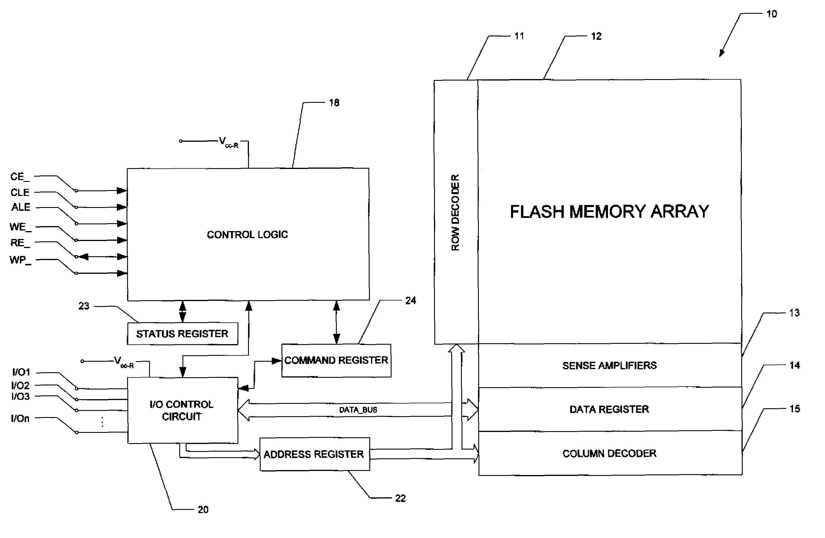
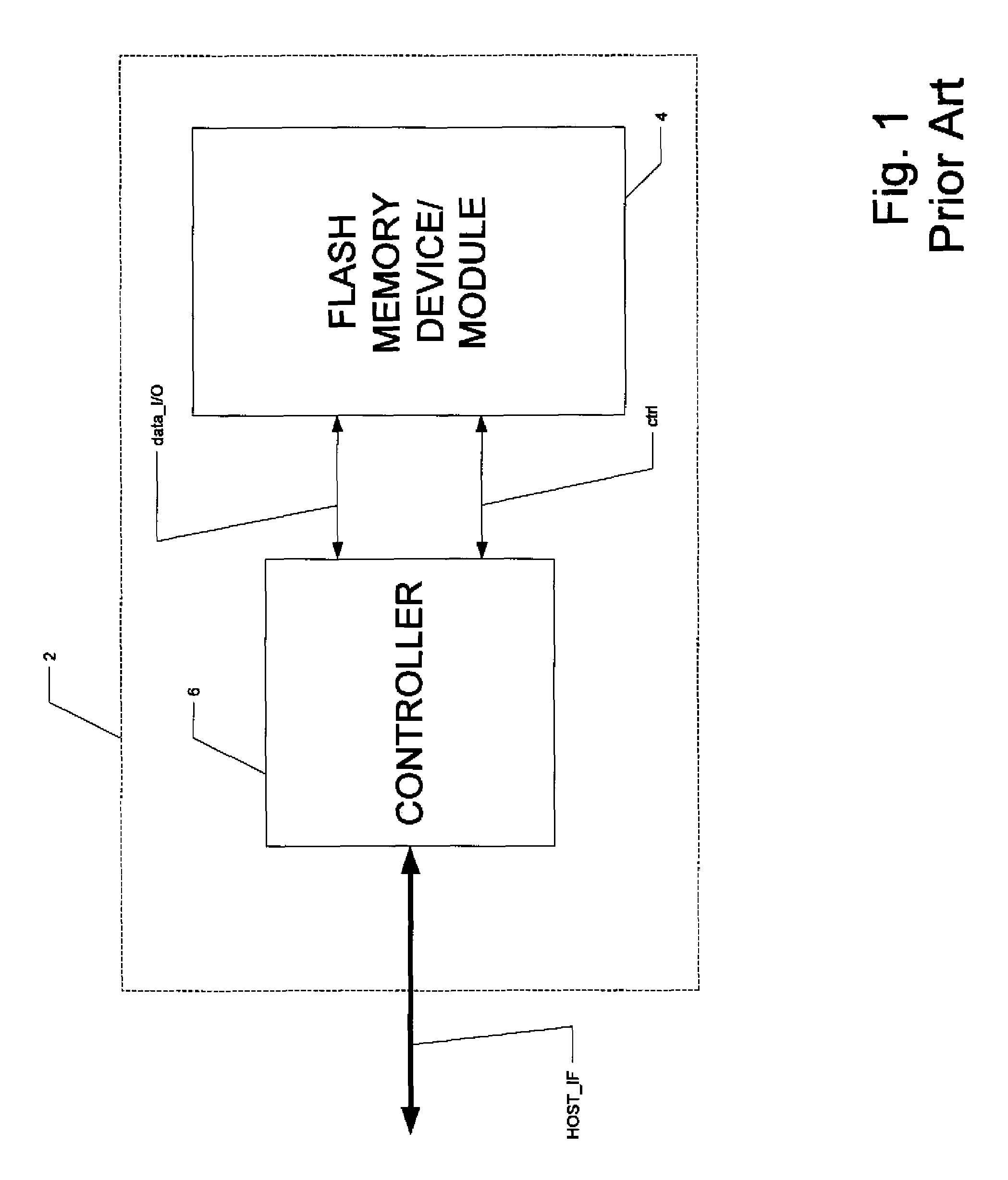
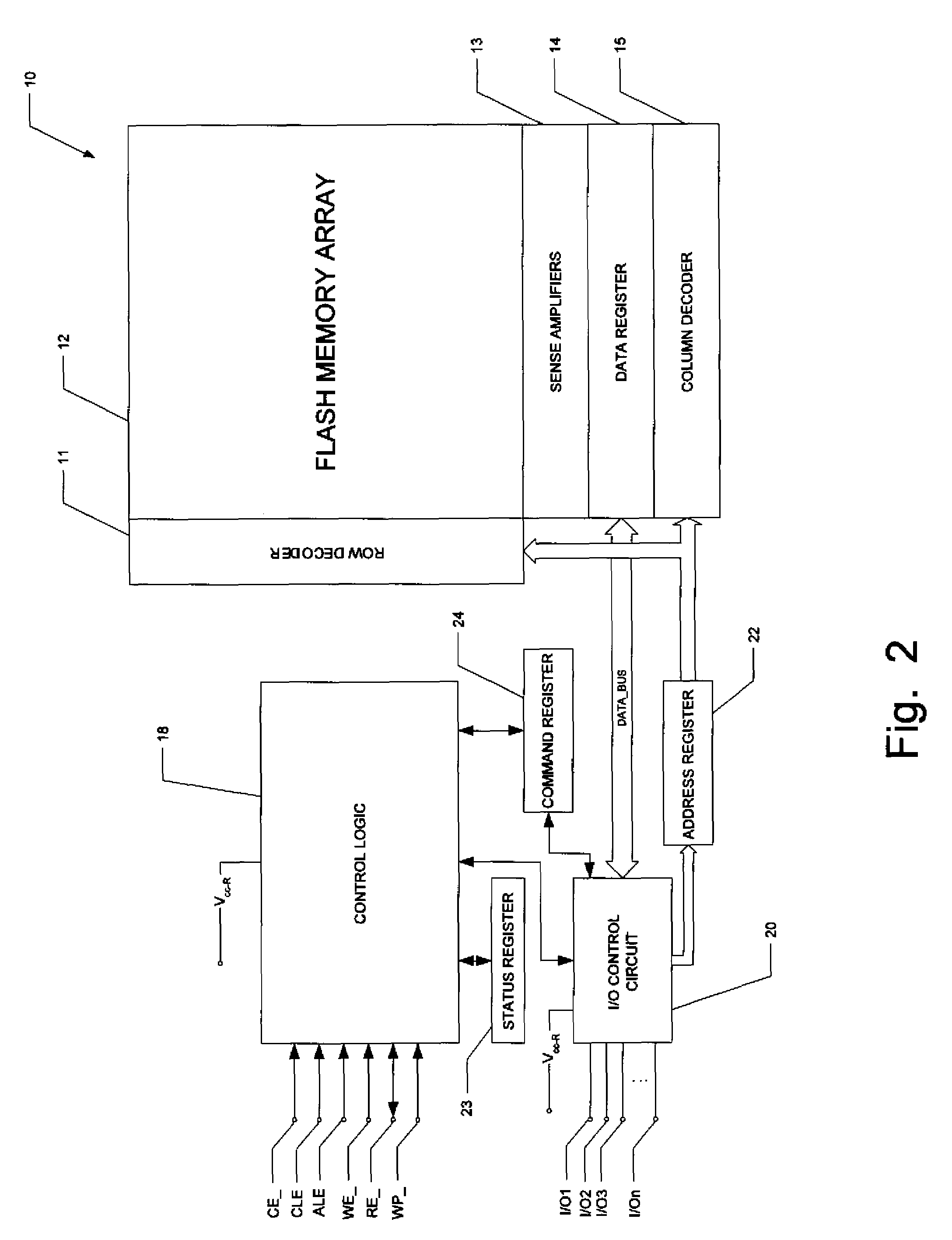
[0027]The present invention will be described in connection with its preferred embodiment, namely as implemented into a flash memory module, and a subsystem including such a flash memory module, and method of operating the same. More specifically, this exemplary flash memory module is described as a multi-level cell (MLC) flash memory of the NAND type, as it is contemplated that this invention will be particularly useful in connection with such flash memories, in order to enable the use of solid-state non-volatile memory for mass data storage in computer systems. However, it is contemplated that this invention will be useful and beneficial in other applications involving non-volatile solid-state memories of various types. Accordingly, it is to be understood that the following description is provided by way of example only, and is not intended to limit the true scope of this invention as claimed.

[0028]FIG. 2 illustrates an exemplary construction of flash memory device (or module) 10 ...


PUM


Abstract

A flash memory system includes a flash memory device and a controller, operable according to an advanced data transfer mode. The flash memory device is operable both in a “legacy” mode, in which read data is presented by the memory synchronously with each cycle of a read data strobe from the controller, and in which input data is latched by the memory synchronously with each cycle of a write data strobe from the controller. In the advanced mode, which can be initiated by the controller forwarding an initiation command to the memory, the flash memory itself sources the read data strobe at a higher frequency, for example at twice the frequency, of that available in the normal mode. In the advanced mode, the input data is presented by the controller synchronously with a higher frequency write data strobe than is available in the normal mode. The voltage swing of the data and control signals is reduced from conventional standards, to reduce power consumption.

Description

CROSS-REFERENCE TO RELATED APPLICATIONS[0001]This application claims priority, under 35 U.S.C. §120, to copending applications Ser. No. 11 / 379,895 filed Apr. 24, 2006, entitled “Method of High-Performance Flash Memory Data Transfer”, and Ser. No. 11 / 379,910, filed Apr. 24, 2006, entitled “High-Performance Flash Memory Data Transfer”, both commonly assigned with this application, and is related to my application Ser. No. 11 / 424,581, filed Jun. 16, 2006, now U.S. Pat. No. 7,366,029, issued Apr. 29, 2008.STATEMENT REGARDING FEDERALLY SPONSORED RESEARCH OR DEVELOPMENT[0002]Not applicable.BACKGROUND OF THE INVENTION[0003]This invention is in the field of flash memory devices, and is more specifically directed to data communications between flash memory devices and memory controllers in electronic systems.[0004]As well known in the art, “flash” memories are electrically-erasable semiconductor memory devices that can be erased and rewritten in relatively small blocks, rather than on a chip...

Claims


Application Information

Patent Timeline
Patent Type & Authority Patents(United States)
IPC IPC(8): G11C7/10
CPCG11C7/1045G11C7/1051G11C7/1066G11C7/1078G11C7/1093G11C7/20G11C7/22G11C11/4099G11C16/102G11C16/26
Inventor KAGAN, YISHAI
Owner SANDISK TECH LLC
Why Eureka
Try Eureka