

Architecture and method for framing optical control and data bursts within optical transport unit structures in photonic burst-switched networks
a technology of optical transport unit and control unit, applied in the field of optical networks, can solve the problems of slow operation, traffic bottleneck of optical switched network, and current optical switch technology cannot efficiently support “bursty” traffi
- Summary
- Abstract
- Description
- Claims
- Application Information
AI Technical Summary
Problems solved by technology
Method used
Image

Examples
Embodiment Construction
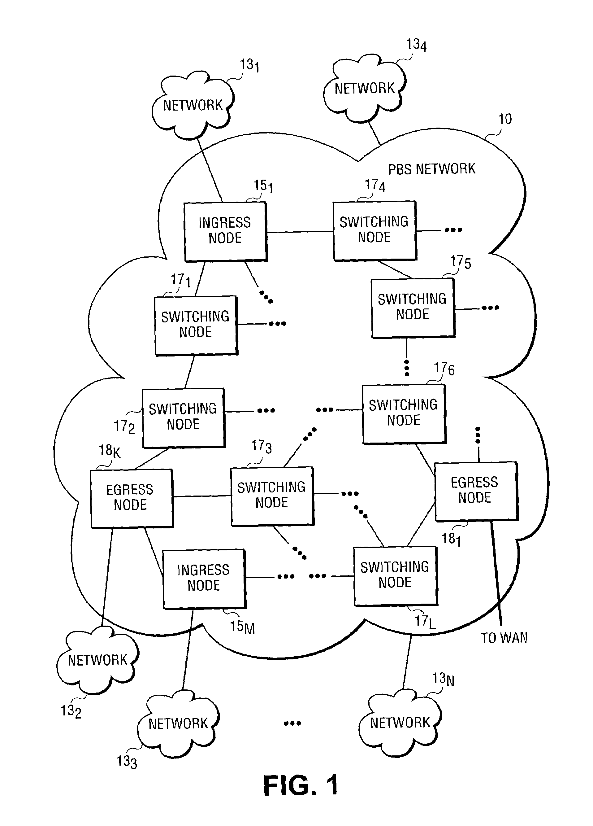
[0021]FIG. 1 illustrates a photonic burst-switched (PBS) network 10, according to one embodiment of the present invention. The term photonic burst is used herein to refer to statistically multiplexed packets (e.g., Internet protocol (IP) packets or Ethernet frames) having similar routing requirements). A photonic burst typically includes a photonic label including the header and other routing information of the IP packets and a payload including the data segments of the packets.
[0022]This embodiment of PBS network 10 is connected to external networks such as local area networks (LANs) 131-13N and a backbone optical WAN (not shown). In addition, this embodiment of PBS network 10 includes ingress nodes 151-15M, switching nodes 171-17L, and egress nodes 181-18K. PBS network 10 can include other ingress, egress and switching nodes (not shown) that are interconnected with the switching nodes shown in FIG. 1. The ingress and egress nodes are also referred to herein as edge nodes in that t...
PUM
 Abstract
Description
Claims
Application Information