Check patentability & draft patents in minutes with Patsnap Eureka AI!

Semiconductor device, method for manufacturing semiconductor device, circuit board, and electronic instrument

a semiconductor device and semiconductor technology, applied in the direction of semiconductor devices, semiconductor/solid-state device details, electrical devices, etc., can solve the problem of easy breakage of the wiring layer

Active Publication Date: 2009-05-05
ADVANCED INTERCONNECT SYST LTD
View PDF21 Cites 13 Cited by
  • Summary
  • Abstract
  • Description
  • Claims
  • Application Information

AI Technical Summary

Benefits of technology

The solution enables the creation of smaller, thinner semiconductor devices with improved connection reliability and high-density packaging, reducing the risk of breakage and allowing for flexible placement of electronic parts, resulting in a more reliable and compact semiconductor device.

Problems solved by technology

However, there is another problem in that breakage easily occurs in the wiring layer due to a stepped portion between the feedthrough electrodes and the semiconductor substrate.

Method used


Image

  • Semiconductor device, method for manufacturing semiconductor device, circuit board, and electronic instrument
  • Semiconductor device, method for manufacturing semiconductor device, circuit board, and electronic instrument
  • Semiconductor device, method for manufacturing semiconductor device, circuit board, and electronic instrument

Examples


Embodiment Construction

[0054]A description will be made as regards a semiconductor device, a method for manufacturing the semiconductor device, a circuit board, and an electronic instrument according to embodiments of the invention.

[0055]First, a description will proceed to the semiconductor device according to an embodiment of the invention.

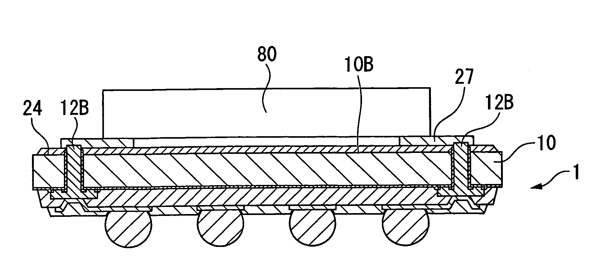
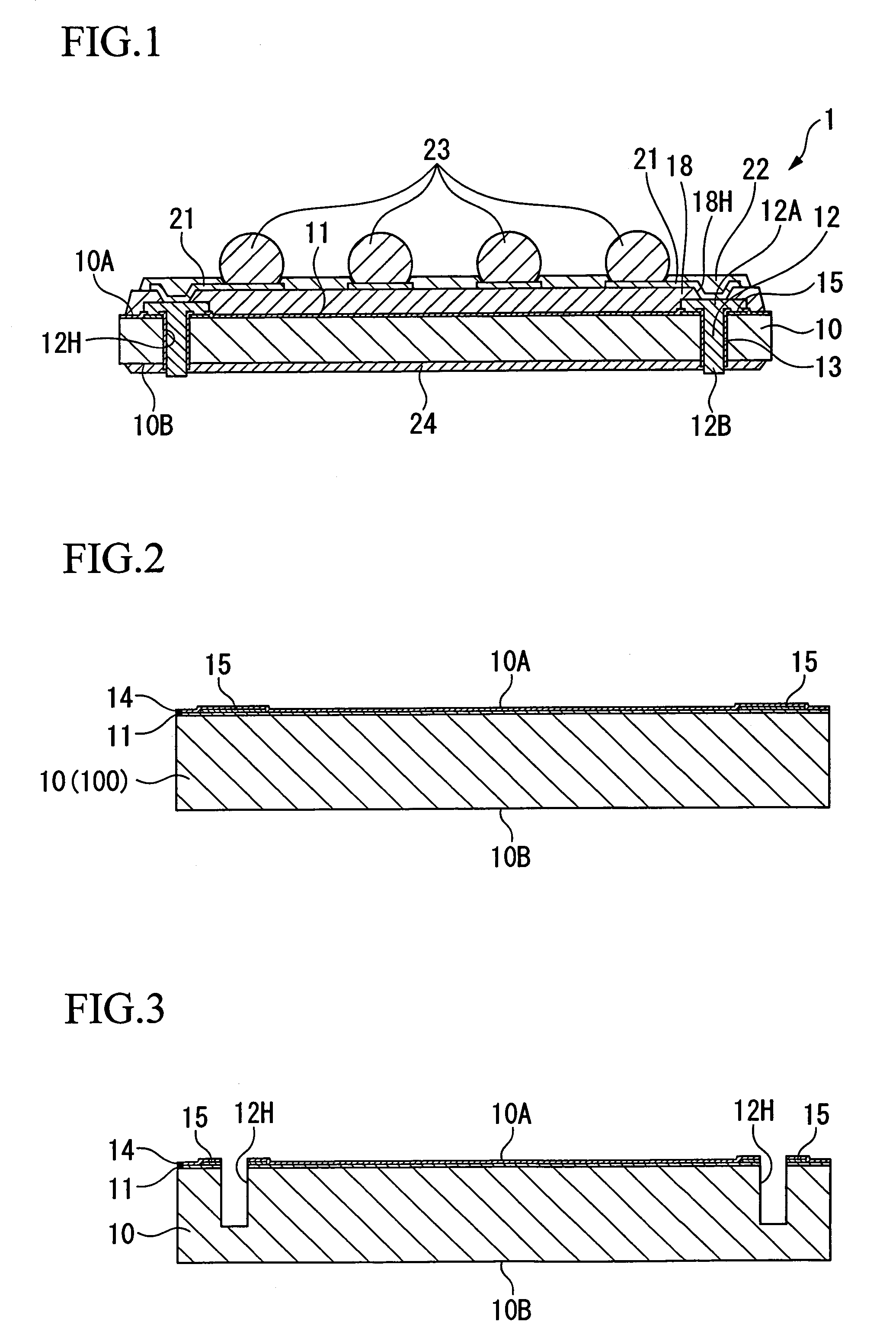
[0056]FIG. 1 is a cross-sectional view illustrating a semiconductor device 1 according to the embodiment. As shown in FIG. 1, the semiconductor device 1 includes a semiconductor substrate 10 composed of a silicon substrate which is obtained by cutting off a silicon wafer. An integrated circuit (not shown) composed of transistors, memory elements, and other electronic elements are formed on an active surface 10A of the semiconductor substrate 10. Feedthrough electrodes 12 are formed in the semiconductor substrate 10 and penetrate from the active surface 10A to a back surface 10B which is opposite to the active surface 10A. In each of the feedthrough electrodes 12 in th...


PUM


Abstract

A semiconductor device includes: a semiconductor substrate having an active surface and a back surface; an integrated circuit formed on the active surface; a feedthrough electrode penetrating the semiconductor substrate, and projecting from the active surface and the back surface; a first resin layer formed on the active surface, having a thickness greater than a height of a portion of the feedthrough electrode that projects from the active surface, and having an opening portion for exposing at least a portion of the feedthrough electrode; a wiring layer which is formed on the first resin layer, and which is connected to the feedthrough electrode through the opening portion; and an external connecting terminal connected to the wiring layer.

Description

[0001]This application claims priority to Japanese Patent Application No. 2004-369081, filed Dec. 21, 2004, the contents of which are incorporated herein by reference.BACKGROUND[0002]1. Technical Field[0003]The present invention relates to a semiconductor device, a method for manufacturing the semiconductor device, a circuit board, and an electronic instrument.[0004]2. Related Art[0005]Recently, electronic parts such as semiconductor devices, which are installed in an electronic instrument, have been downsized in electronic instruments such as a mobile phone, a notebook model personal computer, or a PDA (Personal Data Assistant), with the demand for miniaturization and weight reduction. Under such circumstances, a proposal has been made regarding a three-dimensional packaging technology with respect to the semiconductor device. The three-dimensional packaging technology is for stacking semiconductor devices which have functions similar to one another. In addition, the three-dimensio...

Claims


Application Information

Patent Timeline
Patent Type & Authority Patents(United States)
IPC IPC(8): H01L23/48H01L23/52H01L29/40
CPCH01L21/6835H01L21/76898H01L23/3114H01L23/481H01L24/02H01L24/11H01L24/12H01L24/16H01L24/94H01L25/0657H01L25/50H01L2221/68372H01L2224/0401H01L2224/13009H01L2224/13099H01L2224/13147H01L2224/16H01L2225/06513H01L2225/06524H01L2225/06541H01L2225/06586H01L2924/01002H01L2924/01004H01L2924/01005H01L2924/01013H01L2924/01014H01L2924/01015H01L2924/01022H01L2924/01028H01L2924/01029H01L2924/01033H01L2924/01046H01L2924/01047H01L2924/0105H01L2924/01074H01L2924/01078H01L2924/01079H01L2924/01082H01L2924/014H01L2924/04941H01L2924/05042H01L2924/14H01L2924/15311H01L2924/19041H01L2924/19042H01L2924/19043H01L2924/01006H01L2924/01023H01L2924/01024H01L2224/16146H01L2924/181H01L2224/06181H01L2224/17181H01L2924/0001H01L24/05H01L24/13H01L2224/05548H01L2224/13024H01L2224/02377H01L2224/02372H01L2224/0231H01L2924/00H01L2224/02H01L23/48H01L23/12
Inventor ITO, HARUKI
Owner ADVANCED INTERCONNECT SYST LTD
Features
  • R&D
  • Intellectual Property
  • Life Sciences
  • Materials
  • Tech Scout
  • Unparalleled Data Quality
  • Higher Quality Content
  • 60% Fewer Hallucinations
Learn More