
Semiconductor memory device with ZQ calibration circuit

a technology of zq and memory devices, applied in the field of integrated circuits, can solve the problem that the semiconductor memory device cannot exactly provide the pull-up calculation codes pcal_up

Active Publication Date: 2009-05-05
SK HYNIX INC
View PDF12 Cites 38 Cited by
  • Summary
  • Abstract
  • Description
  • Claims
  • Application Information

AI Technical Summary

Problems solved by technology

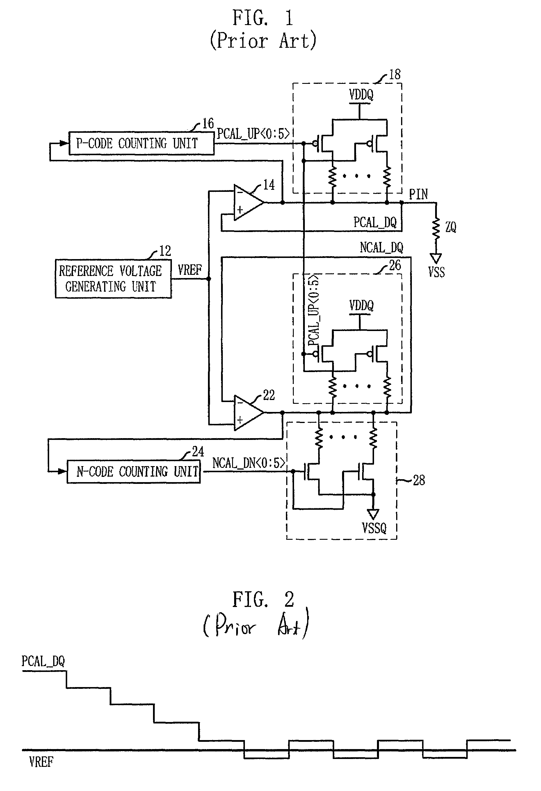
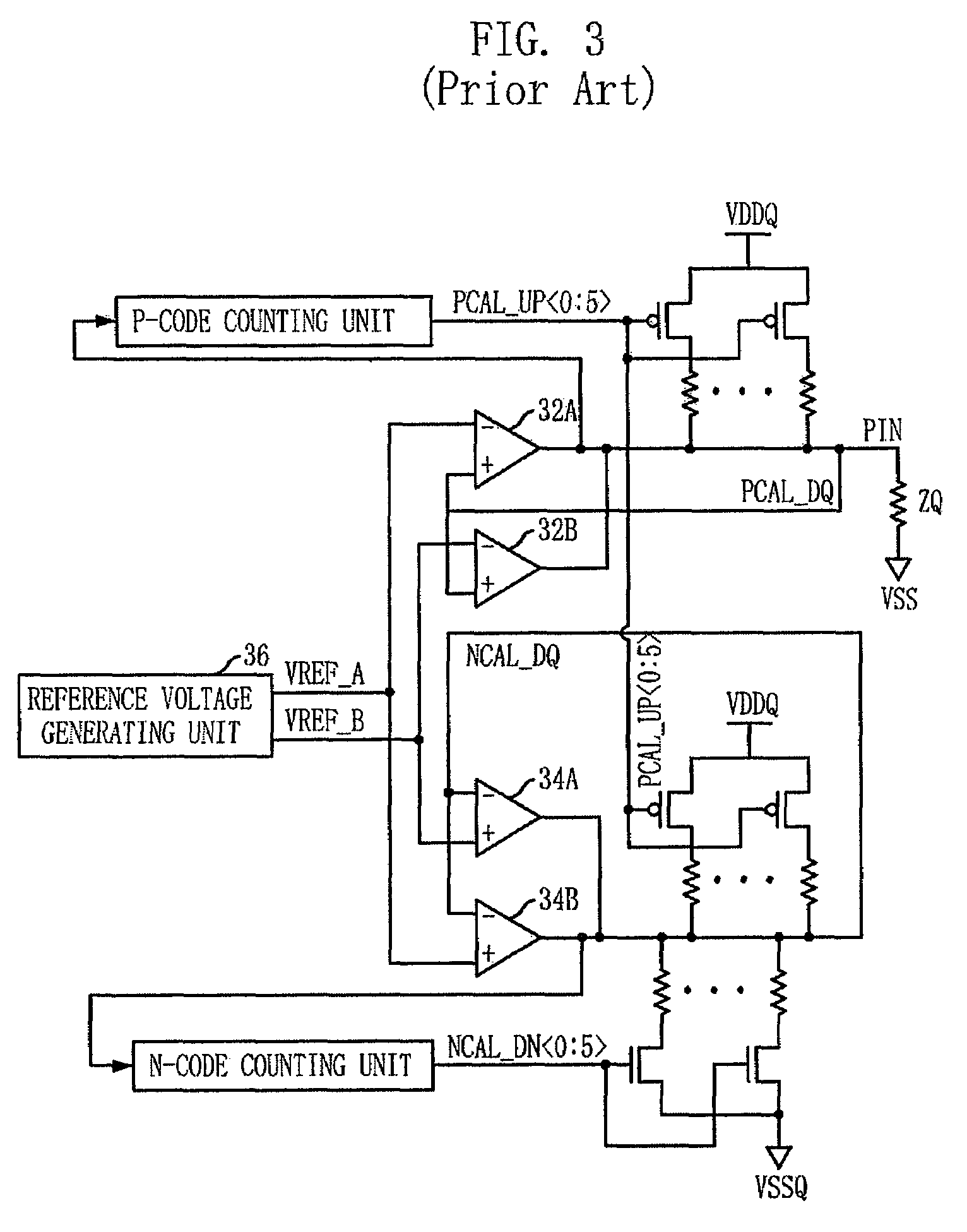
However, in that case, the semiconductor device cannot exactly provide the pull-up calculating codes PCAL_UP0:5> and the pull-down calculating codes NCAL_DN0:5> corresponding to the ZQ resistance.

Method used


Image

  • Semiconductor memory device with ZQ calibration circuit
  • Semiconductor memory device with ZQ calibration circuit
  • Semiconductor memory device with ZQ calibration circuit

Examples


Embodiment Construction

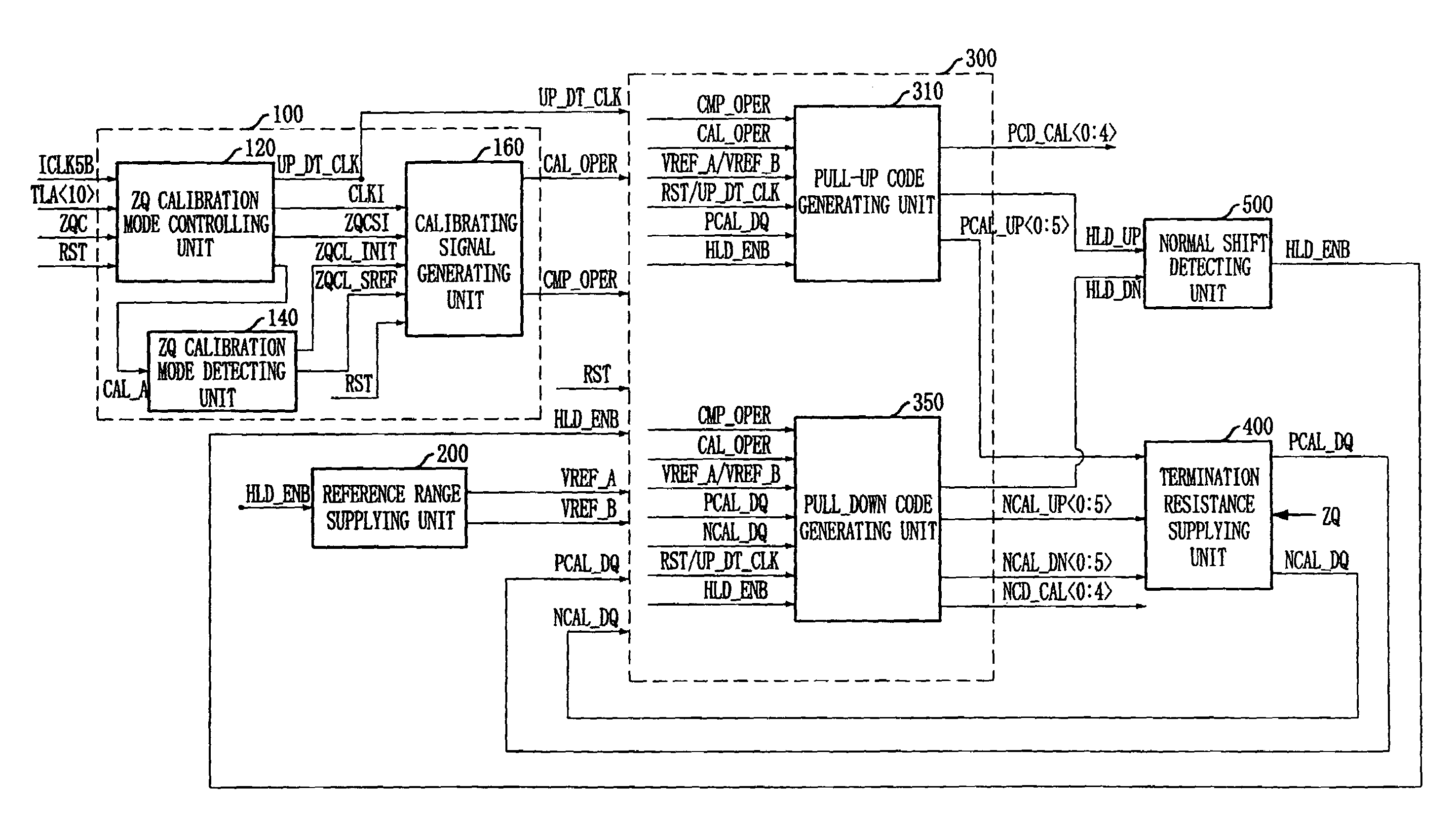
[0048]FIG. 10 shows an exemplary block diagram of a semiconductor memory device according to the present invention. The semiconductor memory device includes a resistance measurement control unit 100, a reference range supplying unit 200, a code generating unit 300, a termination resistance supplying unit 400 and a normal shift detecting unit 500.

[0049]The resistance measurement control unit 100 includes a ZQ calibration mode controlling unit 120, a ZQ calibration mode detecting unit 140 and a calibrating signal generating unit 160. The ZQ calibration mode controlling unit 120 generates a short-calibration signal ZQSCI and a long-calibration signal CAL_A in response to a reset signal RST, a ZQ adjusting signal ZQC and an address TLA10>, and generates a clock signal CLKI and a clock signal UP_DT_CLK using an input clock ICLK5B. The clock signal CLKI is a signal for operating the calibrating signal generating unit 160. The ZQ calibration mode detecting unit 140 generates an initial cal...


PUM


Abstract

An impedance adjusting circuit of semiconductor memory devices is able to adjusting its termination resistance stably. The semiconductor memory device includes a reference range supplying unit for supplying a normal target range corresponding to a ZQ resistance and supplying a micro target range in response to a micro target signal, a termination resistance supplying unit for supplying an output resistance corresponding to a plurality of control codes, a code generating unit for generating the plurality of control codes in order to shift the output resistance within the normal target range and for adjusting the plurality of control codes to shift the output resistance within the micro target range in response to the micro target signal, and a normal shift detecting unit for detecting the output resistance arranged within the normal target range to generate the micro target signal.

Description

CROSS-REFERENCE TO RELATED APPLICATIONS[0001]The present invention claims priority of Korean patent application number 10-2006-0061436, filed on Jun. 30, 2006, which is incorporated by reference in its entirety.BACKGROUND OF THE INVENTION[0002]The present invention relates to integrated circuits, more particular, to an impedance adjusting circuit of semiconductor memory devices.[0003]Generally, semiconductor memory devices including integrated circuits such as a microprocessor, a memory circuit and gate array circuits are used for various electrical appliances, e.g., a personal computer, a server computer and a workstation. The semiconductor memory devices typically include a receiving circuit for receiving signals through input pads from the external and an output circuit for outputting internal signals to the external through output pads. The input / output pads may be connected to a transmission line on a printed circuit board (PCB) on which the semiconductor memory devices are arr...

Claims


Application Information

Patent Timeline
Patent Type & Authority Patents(United States)
IPC IPC(8): H03K17/16
CPCH03K19/0005G11C7/10
Inventor KIM, KI-HO
Owner SK HYNIX INC
Learn More