Semiconductor device semiconductor device testing method, and data processing system

a semiconductor device and semiconductor technology, applied in semiconductor/solid-state device details, generating/distributing signals, instruments, etc., can solve the problems of difficult to speed up the front end unit, difficult to greatly increase the memory capacity of each chip,

Inactive Publication Date: 2011-07-21
LONGITUDE SEMICON S A R L
View PDF7 Cites 59 Cited by
  • Summary
  • Abstract
  • Description
  • Claims
  • Application Information

AI Technical Summary

Benefits of technology

[0011]According to the present invention, in a semiconductor device of a type using an interface chip, it is possible to perform a confirmation test to make sure that there is no consi

Problems solved by technology

Therefore, it is difficult to greatly increase a memory capacity for each chip.
Therefor

Method used


Image

  • Semiconductor device semiconductor device testing method, and data processing system
  • Semiconductor device semiconductor device testing method, and data processing system
  • Semiconductor device semiconductor device testing method, and data processing system

Examples


Embodiment Construction

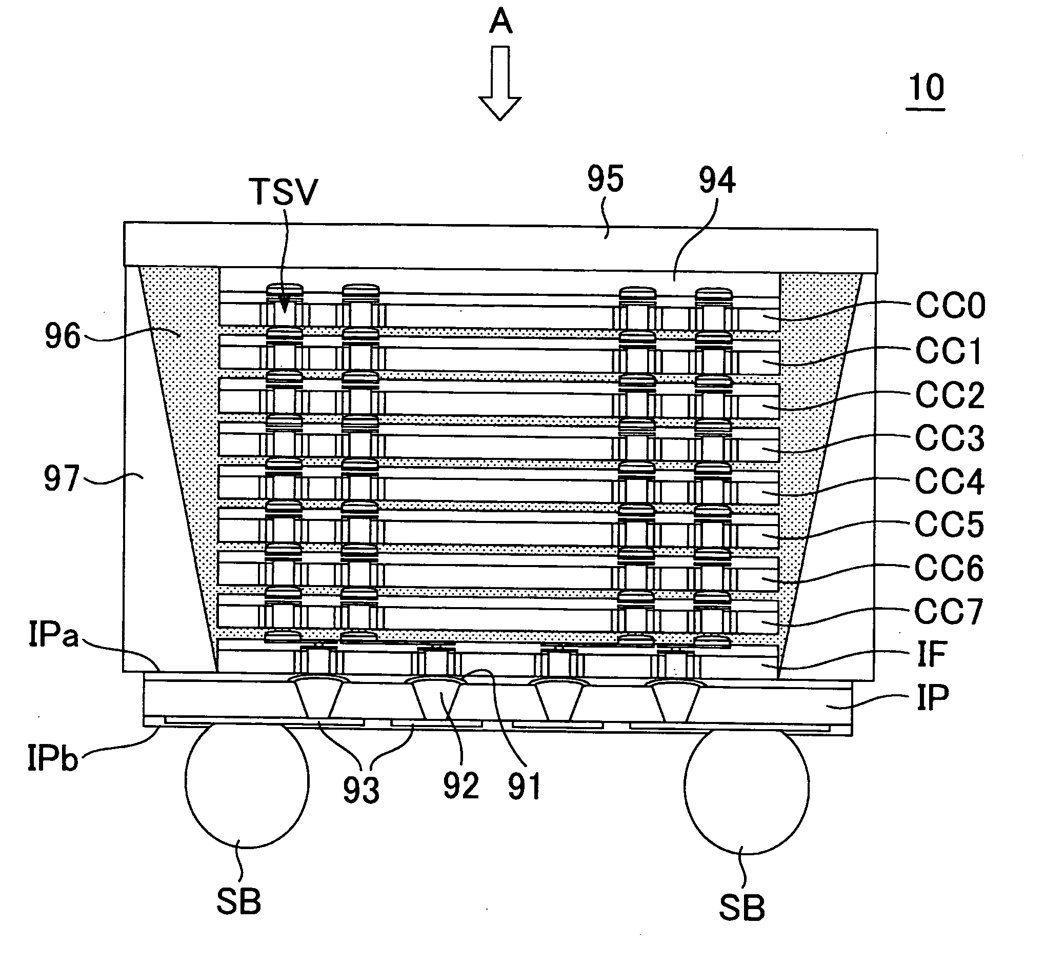
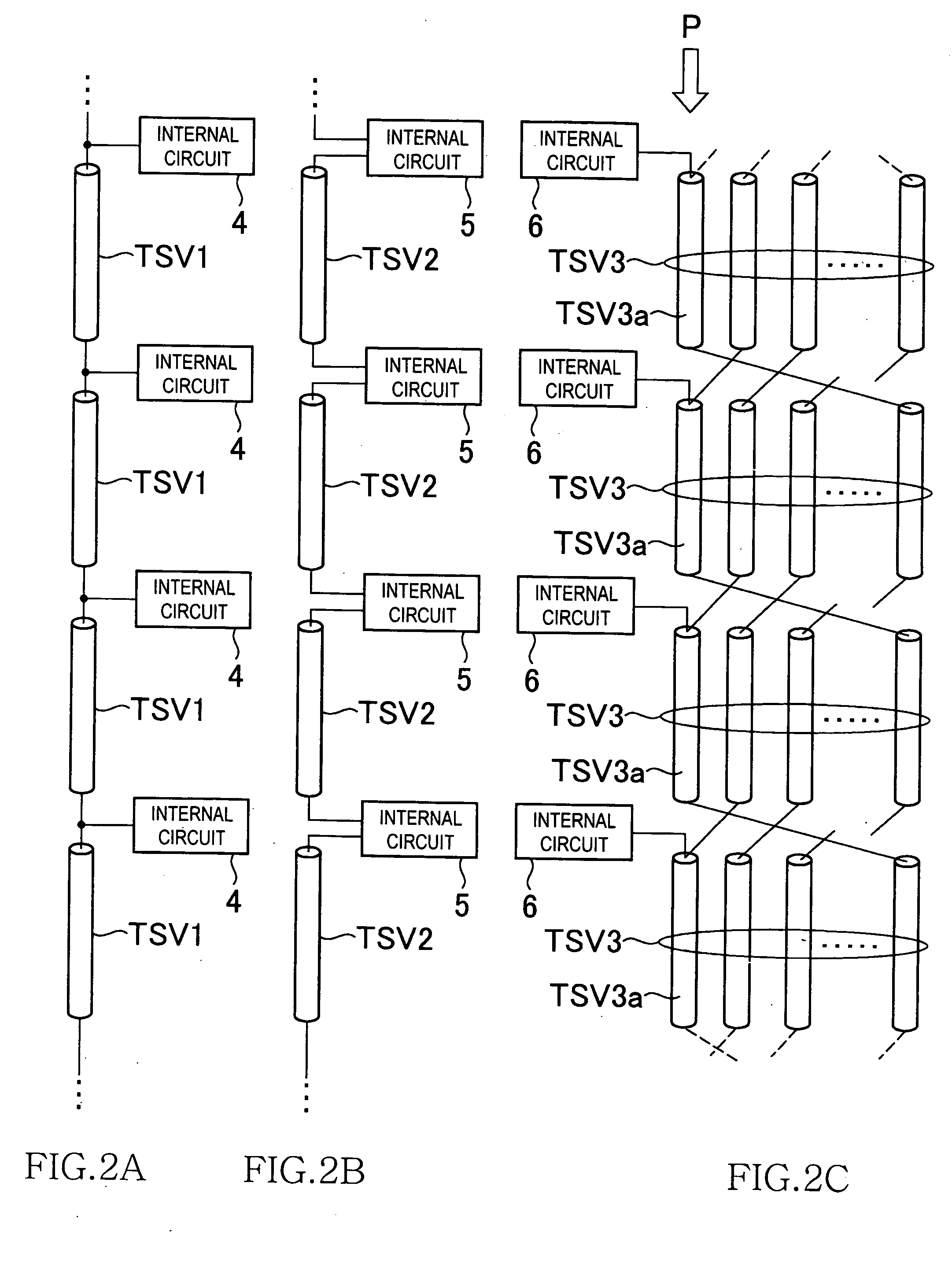
[0022]A representative example of a technical concept for solving the problem of the present invention is described below. It is needless to mention that the contents that the present application is to claim for patent are not limited to the following technical concept, but to the description of the appended claims. That is, the present invention relates to a semiconductor device of a type using an interface chip, which includes a plurality of through silicon vias respectively provided to core chips, and performs a confirmation test to make sure that there is no considerable difference in the delay amount (time constant, AC characteristics) between a measurement-target signal line that electrically connects the interface chip and the core chip and a reference signal line. The interface chip includes a first signal generation circuit that generates a test clock having a predetermined cycle and outputs the test clock to the core chip. The core chip includes a second signal generation ...


PUM


Abstract

To provide a semiconductor device including an interface chip and a core chip and a measurement-target signal line and a reference signal line each including a through silicon via provided in the core chip and electrically connecting the interface chip and the core chip. The interface chip outputs a test clock generated by a first signal generation circuit to the core chip. The core chip includes a second signal generation circuit that generates a predetermined measurement signal from the test clock, and outputs the predetermined measurement signal to the measurement-target signal line and the reference signal line in a simultaneous manner. Further, the interface chip detects a phase difference of a plurality of predetermined measurement signals input via the measurement-target signal line and the reference signal line by an operational amplifier, and outputs a test result to a determination circuit.

Description

BACKGROUND OF THE INVENTION[0001]1. Field of the Invention The present invention relates to a semiconductor device, a semiconductor device testing method, and a data processing system, and more particularly relates to a semiconductor device constituted by a plurality of core chips and an interface chip that controls the core chips, a semiconductor device testing method, and a data processing system.[0002]2. Description of the Related Art[0003]A memory capacity that is required in a semiconductor memory device such as a DRAM (Dynamic Random Access Memory) are increasing every year. To satisfy this requirement, in recent years, a memory device that is called a multi-chip package where plural memory chips are laminated is suggested. However, since the memory chip used in the multi-chip package is a common memory chip capable of operating even though the memory chip is a single chip, a so-called front end unit that performs a function of an interface with an external device (memory cont...

Claims


Application Information

Patent Timeline
IPC IPC(8): G01R31/26H01L23/48
CPCH01L2225/06541H01L2225/06565H01L2924/1305G06F1/12H01L2924/13091H01L2225/06596G11C5/04G11C29/02G11C29/025H01L25/0657H01L2225/06513H01L2225/06517H01L2224/16H01L2224/16145H01L2924/00
Inventor YOKO, HIDEYUKIHARA, KENTAROTAKISHITA, RYUJI
Owner LONGITUDE SEMICON S A R L
Why Eureka
Try Eureka