Design solutions for integrated circuits with triple gate oxides

a technology of triple gate oxide and integrated circuit, which is applied in the field of semiconductor devices, can solve the problems of high standby power consumption, inacceptable products with these devices, and huge increase in leakage currents

Active Publication Date: 2009-05-05
TAIWAN SEMICON MFG CO LTD
View PDF5 Cites 11 Cited by
  • Summary
  • Abstract
  • Description
  • Claims
  • Application Information

AI Technical Summary

Benefits of technology

[0008]By using the embodiments of the present invention, core circuits having different gate dielectric thicknesses can share a common power supply voltage.

Problems solved by technology

However, for ultra-thin silicon dioxide gates, leakage currents will increase tremendously as the thickness is reduced.
This will cause a high standby current in the standby mode (IOFF) and high standby power consumption, thereby making products with these devices commercially unacceptable.
Therefore, reducing standby power consumption and improving performance are often conflicting requirements.
Particularly, problems arise if the high performance circuits and the low standby power-consumption circuits both include static random access memory (SRAM) cells and share a common power supply voltage.
If the desired power supply voltage of high performance circuits, which supply voltage is typically low, is used for both circuits, the SRAM cells in the low standby power-consumption circuits may not be able to function correctly due to inadequate read and / or write margins.
If, however, the power supply voltage is increased to allow the low standby power consumption circuits to work correctly, the power consumption on the high performance circuits is undesirably increased.

Method used


Image

  • Design solutions for integrated circuits with triple gate oxides
  • Design solutions for integrated circuits with triple gate oxides
  • Design solutions for integrated circuits with triple gate oxides

Examples


Embodiment Construction

[0015]The making and using of the presently preferred embodiments are discussed in detail below. It should be appreciated, however, that the present invention provides many applicable inventive concepts that can be embodied in a wide variety of specific contexts. The specific embodiments discussed are merely illustrative of specific ways to make and use the invention, and do not limit the scope of the invention.

[0016]A novel integrated circuit having triple gate oxides and the implementations are illustrated. The variations and operation of the preferred embodiments are then discussed. Throughout the various views and illustrative embodiments of the present invention, like reference numbers are used to designate like elements.

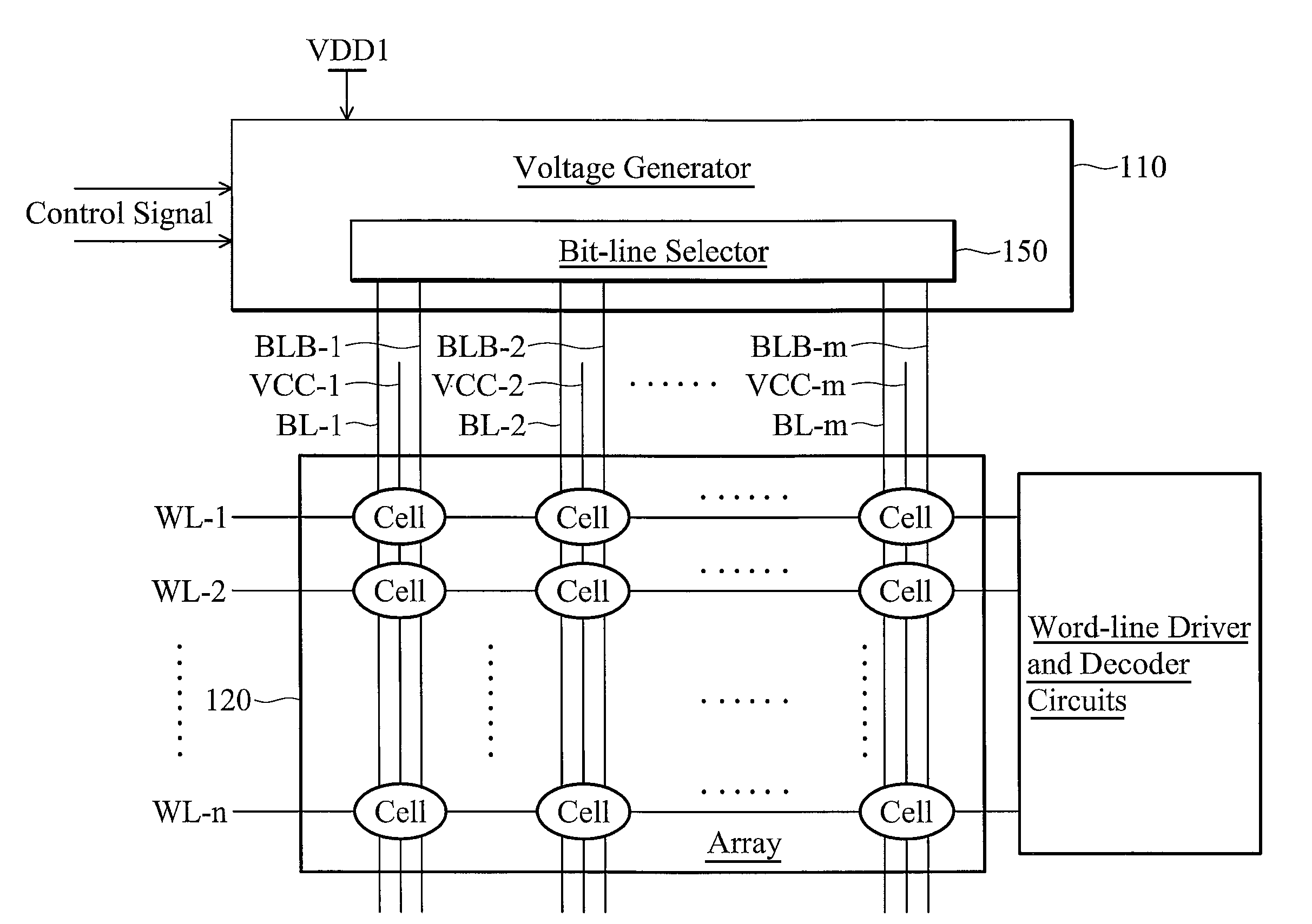
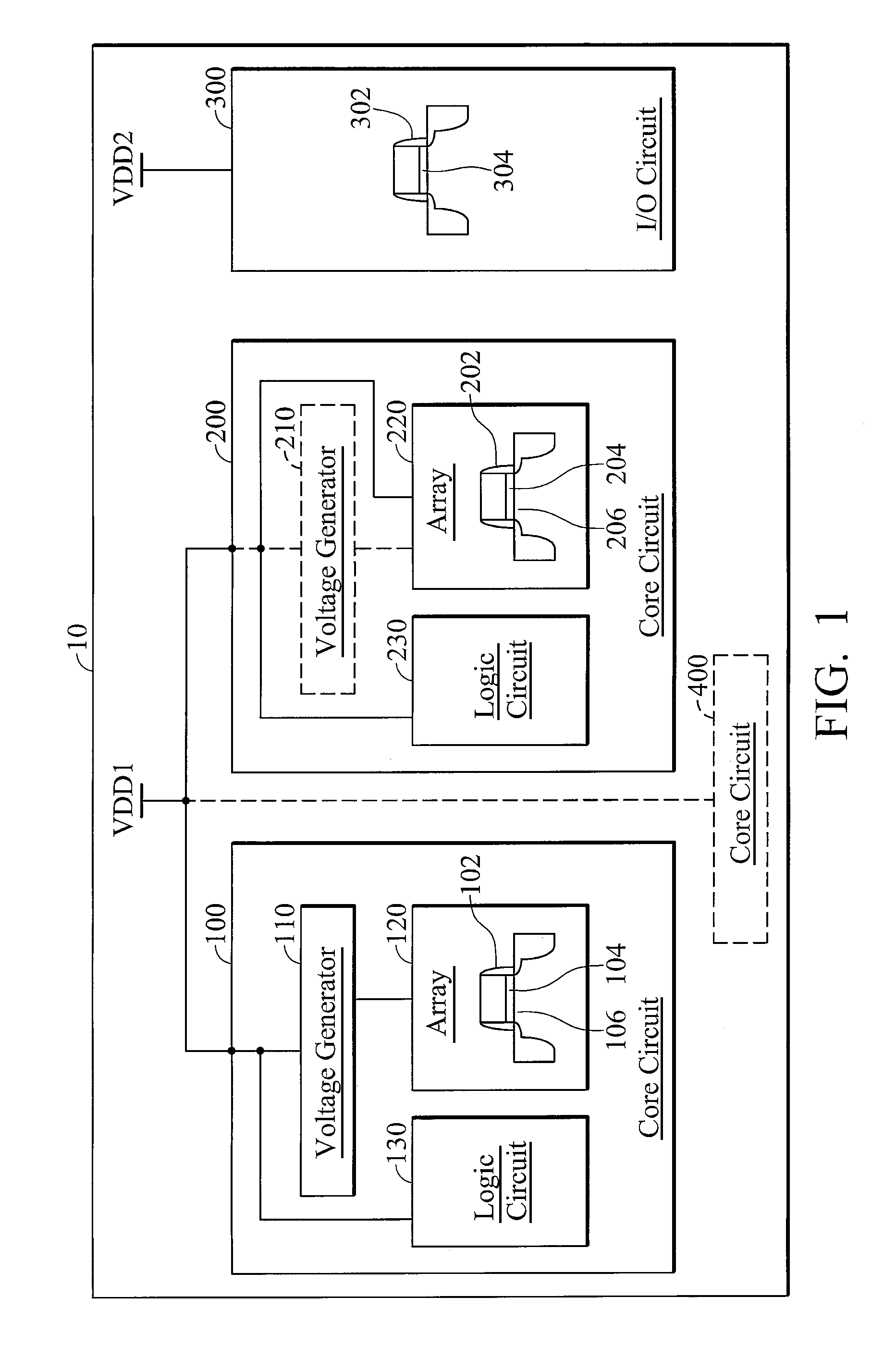
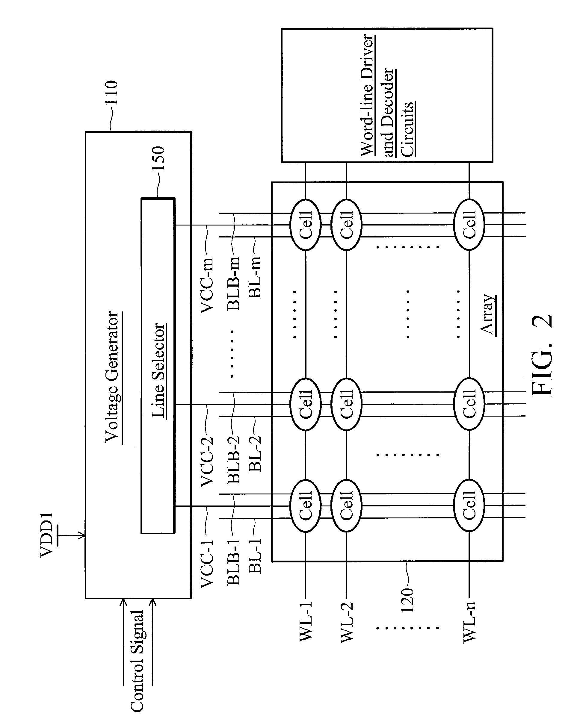
[0017]FIG. 1 schematically illustrates a block diagram of an embodiment of the present invention. A semiconductor chip includes three integrated circuits, core circuit 100, core circuit 200, and input / output (I / O) circuit 300. Preferably, metal-oxide-semiconduc...


PUM


Abstract

An integrated circuit includes a first core circuit and a second core circuits. The first core circuit includes a first MOS device, wherein a first gate dielectric of the first MOS device has a first thickness. The second core circuit includes a second MOS device, wherein a second gate dielectric of the second MOS device has a second thickness less than the first thickness. A first power supply line having a first power supply voltage is connected to the first and the second core circuits a first power supply voltage.

Description

TECHNICAL FIELD[0001]This invention relates generally to semiconductor devices, and more particularly to the formation of integrated circuits having triple gate oxides.BACKGROUND[0002]The thickness of the gate oxides of metal-oxide-semiconductor (MOS) devices is critical to the performance of the MOS devices. There is a constant need for thinner gate oxides to allow for higher-speed devices. Current technology requires gate oxide thicknesses to be about 50 angstroms or less. However, for ultra-thin silicon dioxide gates, leakage currents will increase tremendously as the thickness is reduced. This will cause a high standby current in the standby mode (IOFF) and high standby power consumption, thereby making products with these devices commercially unacceptable. Therefore, reducing standby power consumption and improving performance are often conflicting requirements.[0003]In high end products, there is a need to form devices having multiple gate oxide thicknesses on a same chip. For...

Claims


Application Information

Patent Timeline
Patent Type & Authority Patents(United States)
IPC IPC(8): G11C11/00
CPCG11C5/147G11C11/412G11C11/413H01L27/088
Inventor LIAW, JHON-JHY
Owner TAIWAN SEMICON MFG CO LTD
Why Eureka
Try Eureka