Method of manufacturing nitride-based semiconductor light emitting device

a technology of nitride-based semiconductors and light-emitting devices, which is applied in the field of semiconductor light-emitting devices, can solve the problems of high defect density and limitations to be addressed, and achieve the effect of improving optical output and optical extraction efficiency of nitride-based semiconductor light-emitting devices manufactured according to the present invention

Inactive Publication Date: 2009-05-12
SAMSUNG ELECTRONICS CO LTD
View PDF1 Cites 7 Cited by
  • Summary
  • Abstract
  • Description
  • Claims
  • Application Information

AI Technical Summary

Benefits of technology

[0009]In view of the foregoing deficiencies of the prior art, the present invention provides a method of manufacturing a nitride-based semiconductor light emitting device having an improved structure in which optical extraction efficiency is improved.
[0011]In another embodiment, a photophysical mass transport phenomenon of azobenzene-functionalized polymer is used such that a nitride-based semiconductor light-emitting device having a plurality of photonic crystal arrays is manufactured. Accordingly, optical output and optical extraction efficiency in the nitride-based semiconductor light-emitting device manufactured according to the present invention can be improved as compared to the prior art.

Problems solved by technology

However, in such LEDs, defect density is high due to limitations of manufacture technology.
Thus, limitations to be addressed in the current technical objectives include improving internal quantum efficiency of an MQW layer, and manufacturing a high-power LED.

Method used


Image

  • Method of manufacturing nitride-based semiconductor light emitting device
  • Method of manufacturing nitride-based semiconductor light emitting device
  • Method of manufacturing nitride-based semiconductor light emitting device

Examples


Embodiment Construction

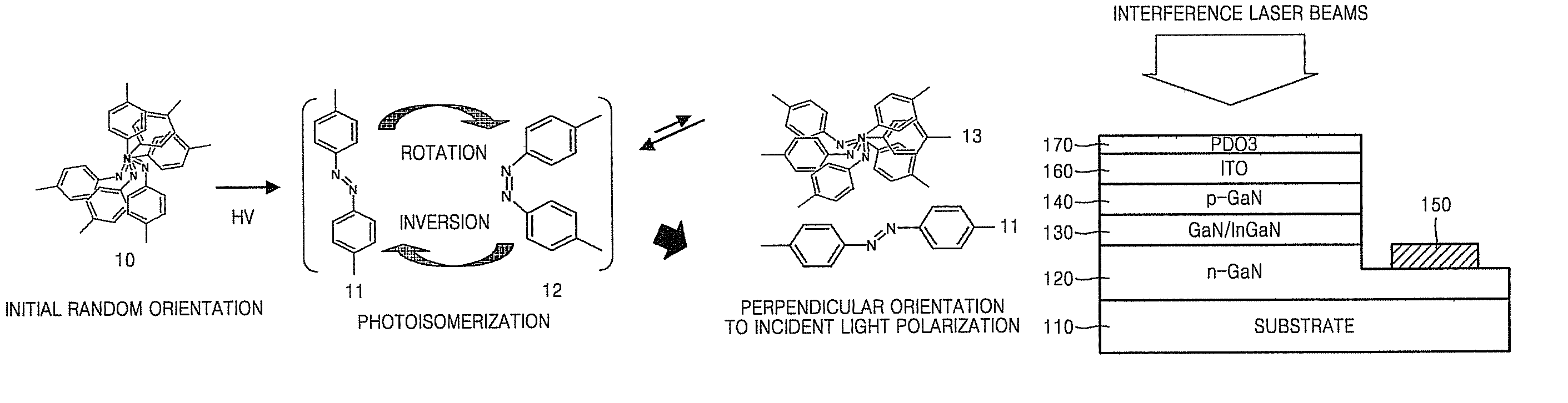
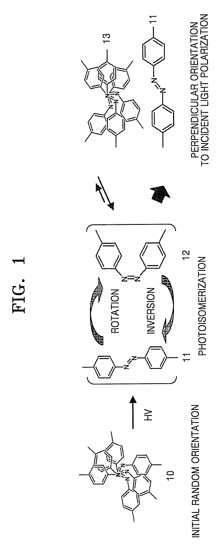
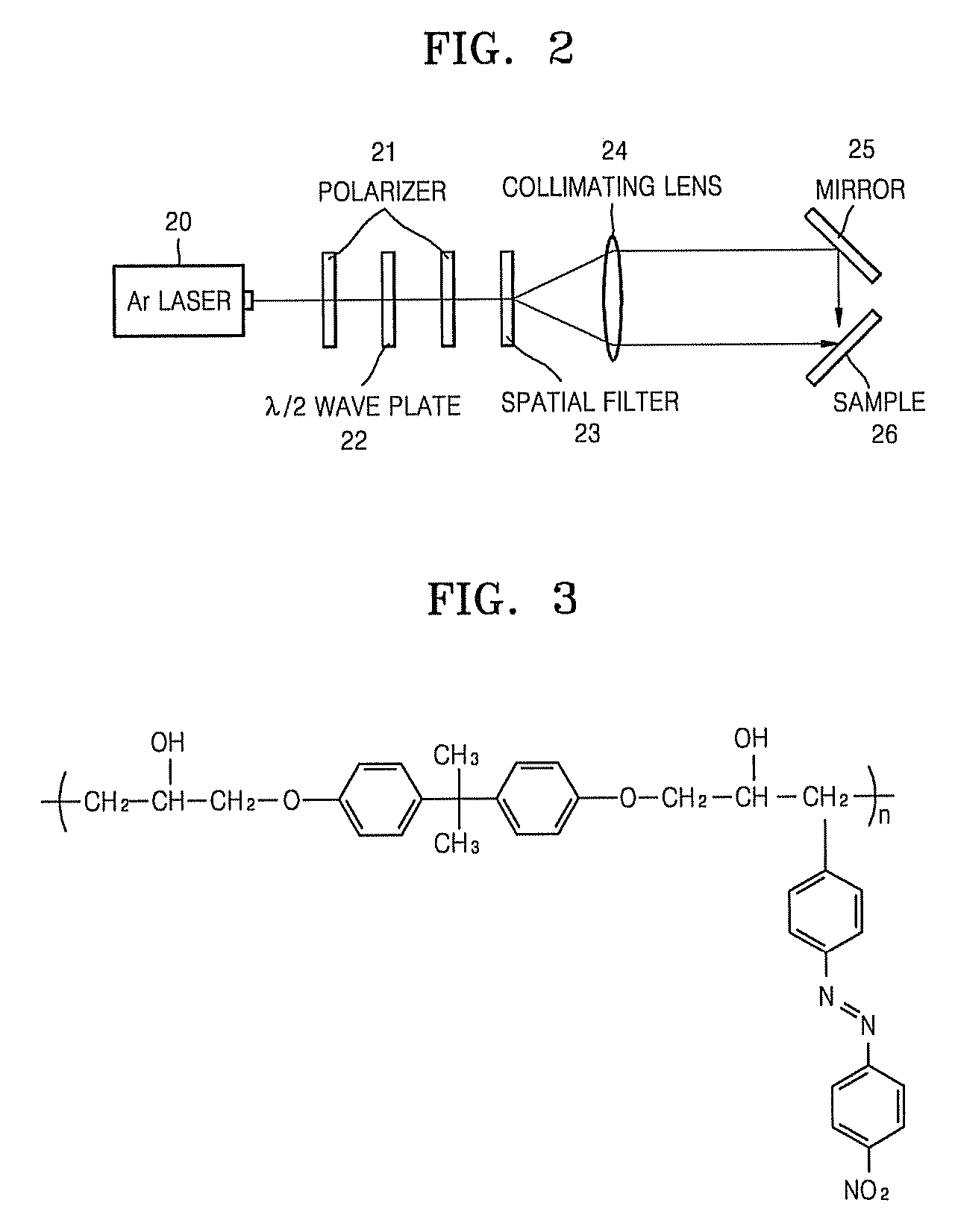
[0020]The present invention will now be described more fully with reference to the accompanying drawings, in which exemplary embodiments of the invention are shown. In the drawings, the thicknesses of layers and regions are exaggerated for clarity.

[0021]It will be understood that when an element is referred to as being “on” another element, it can be directly on the other element or intervening elements may be present therebetween. In contrast, when an element is referred to as being “disposed on” another element, the elements are understood to be in at least partial contact with each other, unless otherwise specified.

[0022]The terminology used herein is for the purpose of describing particular embodiments only and is not intended to be limiting of the invention. As used herein, the singular forms “a”, “an” and “the” are intended to include the plural forms as well, unless the context clearly indicates otherwise. It will be further understood that the terms “comprises” and / or “compr...


PUM


Abstract

Provided is a method of manufacturing a nitride-based semiconductor light-emitting device having an improved structure in which optical extraction efficiency is improved. The method of manufacturing a nitride-based semiconductor light-emitting device including an n-doped semiconductor layer, an active layer, a p-doped semiconductor layer, an n-electrode and a p-electrode includes: forming an azobenzene-functionalized polymer film on a base layer by selecting one layer from the group consisting of the n-doped semiconductor layer, the p-doped semiconductor layer, the n-electrode and the p-electrode as the base layer; forming surface relief gratings of a micro-pattern caused by a photophysical mass transport property of azobenzene-functionalized polymer by irradiating interference laser beams onto the azobenzene-functionalized polymer film; forming a photonic crystal layer using a metal oxide on a recessed gap of the azobenzene-functionalized polymer film, and removing the azobenzene-functionalized polymer film.

Description

[0001]This application claims priority to Korean Patent Application No. 10-2006-0045112, filed on May 19, 2006, and all the benefits accruing therefrom under 35 USC § 119(a), the content of which is incorporated herein by reference in its entirety.BACKGROUND OF THE INVENTION[0002]1. Field of the Invention[0003]The present invention relates to a semiconductor light emitting device, and more particularly, to a method of manufacturing a nitride-based semiconductor light emitting device having an improved structure in which optical extraction efficiency is improved.[0004]2. Description of the Related Art[0005]Light emitting devices, such as light emitting diodes (“LEDs”), are generally semiconductor p-n junction diodes. Silicon p-n junctions continue to play a leading role in the electronic information revolution, and p-n junctions of a group III-V semiconductor continue to play a leading role in the optical revolution away from traditional incandescent or fluorescent light sources and ...

Claims


Application Information

Patent Timeline
Patent Type & Authority Patents(United States)
IPC IPC(8): H01L21/31H01L33/22H01L33/36
CPCH01L33/22H01L33/0095H01L33/42
Inventor CHO, JAE-HEESONE, CHEOL-SOOKIM, DONG-YUHONG, HYUN-GIKIM, SEOK-SOON
Owner SAMSUNG ELECTRONICS CO LTD
Why Eureka
Try Eureka