Multi-channel thin film transistor structure

a thin film transistor and multi-channel technology, applied in the direction of transistors, electrical devices, semiconductor devices, etc., can solve the problems of reducing the threshold voltage shift, the display is prone to serious effects of threshold voltage shift, so as to reduce the threshold voltage shift

Active Publication Date: 2009-05-12
E INK HLDG INC
View PDF15 Cites 12 Cited by
  • Summary
  • Abstract
  • Description
  • Claims
  • Application Information

AI Technical Summary

Benefits of technology

[0017]According to the preferred embodiments mentioned above, the multi-channel TFT of the present invention has a plurality of parallel semiconductor islands to split the source-drain current into several parts. Thus, the threshold voltage shift of the multi-channel TFT can be reduced. Moreover, locating the semiconductors two abreast can further reduce the threshold voltage shift. Further, the multi-channel TFT of the present invention can be in the form of a bottom gate TFT or a top gate TFT. The semiconductor island can be made of amorphous silicon (a-Si). Hence, the multi-channel TFT of the present invention can be widely used.

Problems solved by technology

The threshold voltage shift may cause a decrease of the source-drain current and quality degradation of displays.
The threshold voltage shift due to the interface degradation may result in a decrease of the source-drain current and quantity reduction of the displays.
The threshold voltage shift has a serious effect on displays.
Therefore, how to provide a thin film transistor structure to reduce the threshold voltage shift is an issue of great consequence.

Method used


Image

  • Multi-channel thin film transistor structure
  • Multi-channel thin film transistor structure
  • Multi-channel thin film transistor structure

Examples


Embodiment Construction

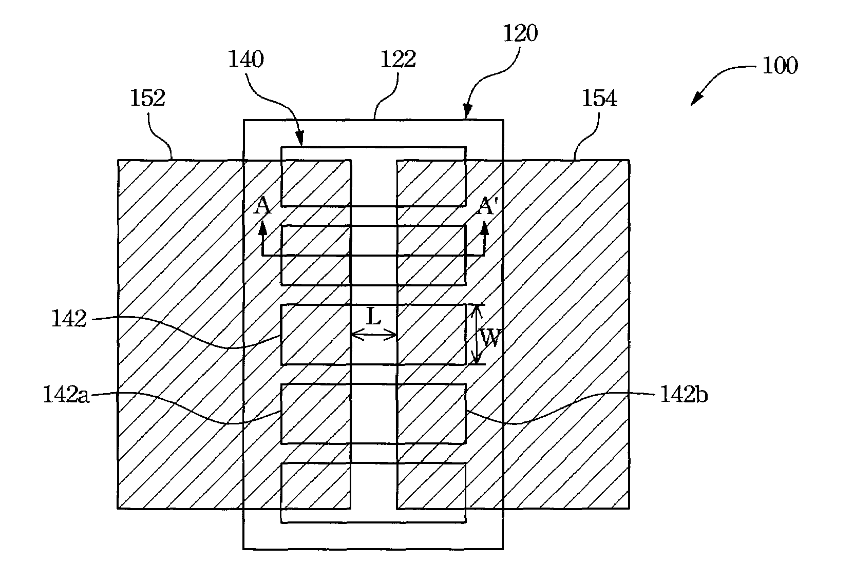
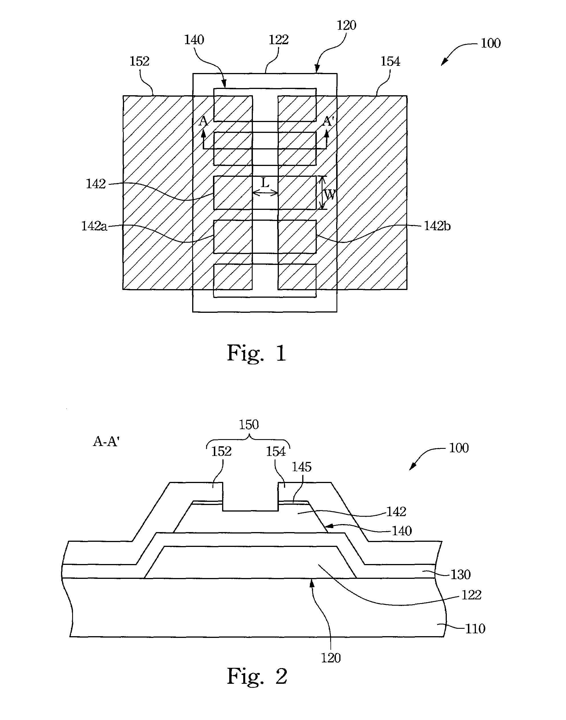
[0026]FIG. 1 illustrates a bottom gate TFT according to the preferred embodiment of the present invention. FIG. 2 illustrates a cross-sectional view from the A-A′ line in FIG. 1. Referring to FIG. 1 and FIG. 2, the TFT 100 can be a lo driving TFT of an OLED display or a PLED display. The TFT 100 includes a first conducting layer 120, an insulating layer 130, a semiconductor layer 140 and a second conducting layer 150. The first conducting layer 120 formed on a substrate 110 includes a gate electrode 122. The insulating layer 130 covers the first conducting layer 120. The semiconductor layer 140 is formed on the insulating layer 130. The semiconductor layer 140 includes a plurality of semiconductor islands 142 located above the gate electrode 122. The second conducting layer 150 is formed on the insulating layer 130 and on the semiconductor layer 140. The second conducting layer 150 includes a source electrode 152 and a drain electrode 154. A contact layer 145 is formed between the s...


PUM


Abstract

A multi-channel thin film transistor structure including a first conducting layer, an insulating layer, a semiconductor layer and a second conducting layer is provided. The first conducting layer formed on a substrate includes a gate electrode. The insulating layer covers the first conducting layer. The semiconductor layer formed on the insulating layer includes a plurality of semiconductor islands located above the gate electrode. The second conducting layer formed on the insulating layer and on the semiconductor layer includes a source electrode and a drain electrode. Each one of the semiconductor islands is coupled electrically with the source electrode at one end and coupled electrically with the drain electrode at the other end.

Description

RELATED APPLICATIONS[0001]The present application is based on, and claims priority from, Taiwan Application Serial Number 95116147, filed May 5, 2006, the disclosure of which is hereby incorporated by reference herein in its entirety.BACKGROUND[0002]1. Field of Invention[0003]The present invention relates to a thin film transistor structure, and more particularly, to a multi-channel thin film transistor structure.[0004]2. Description of Related Art[0005]There are two types of display architectures: passive matrix and active matrix. In general, a thin film transistor (TFT) can be used as a switching element to control each pixel individually in active matrix type displays. A threshold voltage shift of a TFT may occur due to a continuing positive bias stress or a positive bias stress with heavy-duty circle supplied at the TFT gate electrode. The threshold voltage shift may cause a decrease of the source-drain current and quality degradation of displays.[0006]In organic light emitting ...

Claims


Application Information

Patent Timeline
Patent Type & Authority Patents(United States)
IPC IPC(8): H01L27/13
CPCH01L29/78696H01L29/41733H01L29/78669
Inventor LIU, CHUAN-FENG
Owner E INK HLDG INC
Why Eureka
Try Eureka