Switch circuit

a switch circuit and circuit technology, applied in the field of switch circuits, can solve the problems of consuming a larger power under a low resistance, poor compatibility of pin diodes with heterojunction transistors, and not yet available reports regarding circuits including microstrip lines, etc., to maximize the isolation of the branch path, suppress the effect of insertion loss, and maximize the isolation of the off branch

Inactive Publication Date: 2009-05-12
RENESAS ELECTRONICS CORP
View PDF10 Cites 6 Cited by
  • Summary
  • Abstract
  • Description
  • Claims
  • Application Information

AI Technical Summary

Benefits of technology

[0021]In the switch circuit thus configured, the transmission line is longer than 45% of Λ / 4 but shorter than Λ / 4. The transmission line longer than 45% of Λ / 4 allows suppressing the insertion loss in an ON state within a tolerance. Also, the transmission line shorter than Λ / 4 enables maximizing the isolation of the branch path under an OFF state.
[0022]Thus, the present invention provides a switch circuit appropriate for maximizing the isolation of the OFF branch and suppressing the insertion loss in an ON state within a tolerance.

Problems solved by technology

The PIN diode has poor compatibility with a heterojunction transistor process to constitute most of millimeter-wave monolithic integrated circuit (MMIC), and consumes a larger power under a low resistance.
A report on the SPnT switch including the distributed constant FET, however, can only be found in a circuit including a coplanar waveguide reviewed hereunder, and no report is available yet regarding a circuit including a microstrip line.
Such circuit is, despite being popularly utilized, difficult to achieve a high isolation characteristic in the broadband.

Method used


Image

  • Switch circuit
  • Switch circuit
  • Switch circuit

Examples


Embodiment Construction

[0046]The invention will be now described herein with reference to illustrative embodiments. Those skilled in the art will recognize that many alternative embodiments can be accomplished using the teachings of the present invention and that the invention is not limited to the embodiments illustrated for explanatory purposes.

[0047]Hereunder, exemplary embodiments of a semiconductor device and a method of manufacturing the same according to the present invention will be described in details, referring to the accompanying drawings. In the drawings, same constituents are given the identical numerals, and duplicating description may not be repeated where appropriate.

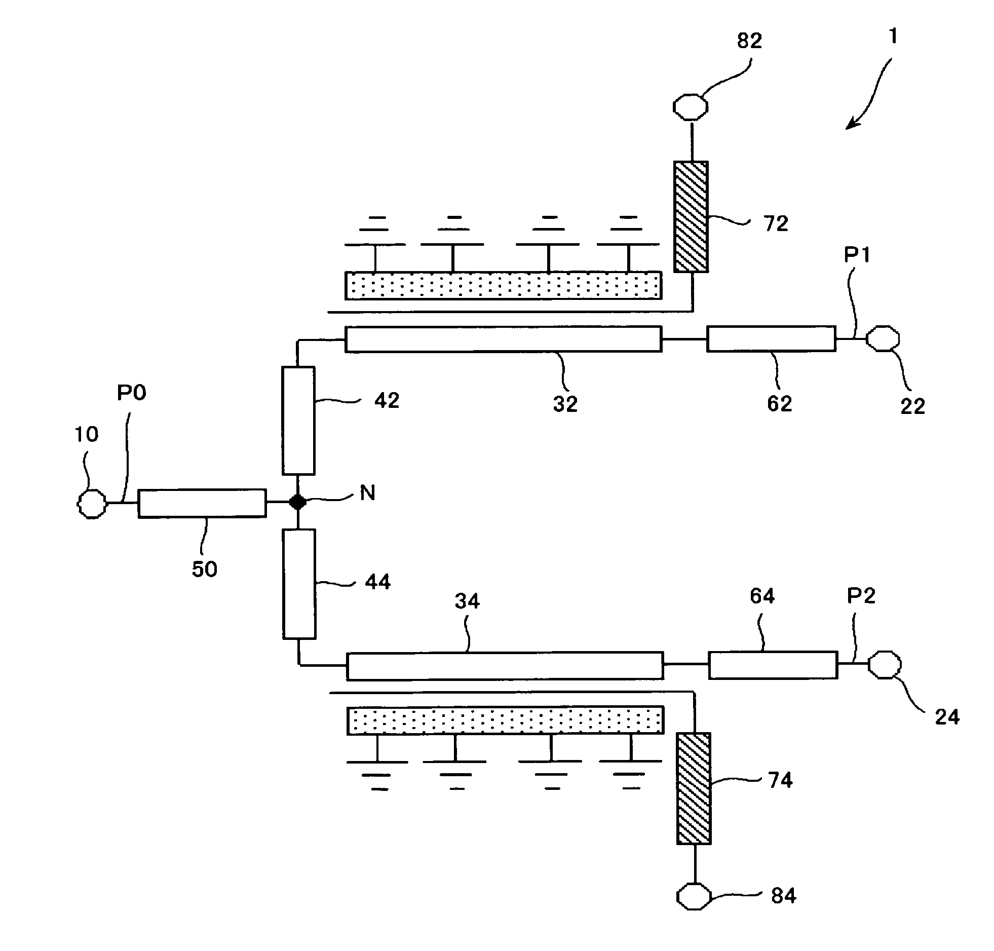
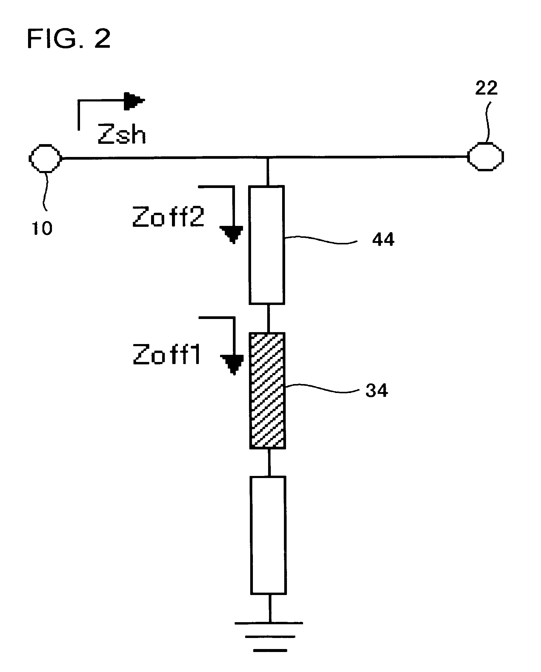
[0048]FIG. 1 is a circuit diagram of a switch circuit according to an embodiment of the present invention. The switch circuit 1 is a traveling wave type SPDT switch including distributed constant FETs, applicable to, for example, a system for a microwave band and a millimeter-wave band. The switch circuit 1 includes a common ...


PUM


Abstract

The switch circuit 1 includes a common terminal 10 (common port), a plurality of branch terminals 22, 24, a common path P0 connecting the common terminal 10 and a diverging point N, branch paths P1, P2 connecting the diverging point N and the branch terminals 22, 24 respectively, distributed constant FETs 32, 34 respectively provided in the branch paths P1, P2, and transmission lines 42, 44 provided between the diverging point N on the branch paths P1, P2 and the distributed constant FETs 32, 34 respectively. Here, the transmission lines 42, 44 are longer than 45% of Λ / 4 but shorter than Λ / 4, when Λ designates a propagation wavelength under an operating frequency.

Description

[0001]This application is based on Japanese patent application No. 2005-221147, the content of which is incorporated hereinto by reference.BACKGROUND[0002]1. Technical Field[0003]The present invention relates to a switch circuit.[0004]2. Related Art[0005]Active elements employed in a switch circuit that operates under a microwave band or a millimeter-wave band (millimeter-wave band covers a range of 30 GHz to 300 GHz) include a PIN diode and a field effect transistor (hereinafter, FET), each of which has its characteristics. In particular, to reduce insertion loss and improve isolation performance it is essential to reduce ON resistance and OFF capacitance of the active element, for which the PIN diode is more superior. In many of the millimeter-wave switch circuits of 30 GHz or higher especially, the PIN diode is employed for reducing the resistance and the capacitance. The PIN diode is, however, inferior to the FET in the following aspects. The PIN diode has poor compatibility wit...

Claims


Application Information

Patent Timeline
Patent Type & Authority Patents(United States)
IPC IPC(8): H01P1/15
CPCH01P1/15
Inventor MIZUTANI, HIROSHI
Owner RENESAS ELECTRONICS CORP
Why Eureka
Try Eureka