Differential offset spacer

a technology of offset spacer and offset spacer, which is applied in the field of semiconductor device processing, can solve the problems of significant variability in transistors, degrade the stability of sram bit cells, and the conventional single spacer process does not provide flexibility with respect to the application/function of a given transistor (e.g. high voltage or speed),

Active Publication Date: 2009-05-26
TEXAS INSTR INC
View PDF5 Cites 8 Cited by
  • Summary
  • Abstract
  • Description
  • Claims
  • Application Information

AI Technical Summary

Problems solved by technology

Although a single spacer structure simplifies the process flow, a conventional single spacer process does not provide flexibility with respect to the application / function for a given transistor (e.g. high voltage or speed), nor the type of transistor (e.g. PMOS or NMOS).
Items (i)-(iii) are known to impact SRAM bit cell transistor mismatch (local variation) which can degrade SRAM bit cell stability.
Non-uniformity in underlying / remaining oxide thickness can cause significant variability in transistors formed post offset spacer etch.
However, as dimensions are reduced to scale down devices, it becomes increasingly difficult to achieve a balance in the relative strengths (e.g. drive current capability) of the pass gate, drive, and load transistors over the desired range of temperature, bias conditions, and process variations, as well as achieving matched transistor characteristics.
As a result, SRAM cells formed as such can be adversely affected by varying operating characteristics and may be unstable and may not be able to retain the desired bit state, during either or both the read or write operations.

Method used


Image

  • Differential offset spacer
  • Differential offset spacer
  • Differential offset spacer

Examples


Embodiment Construction

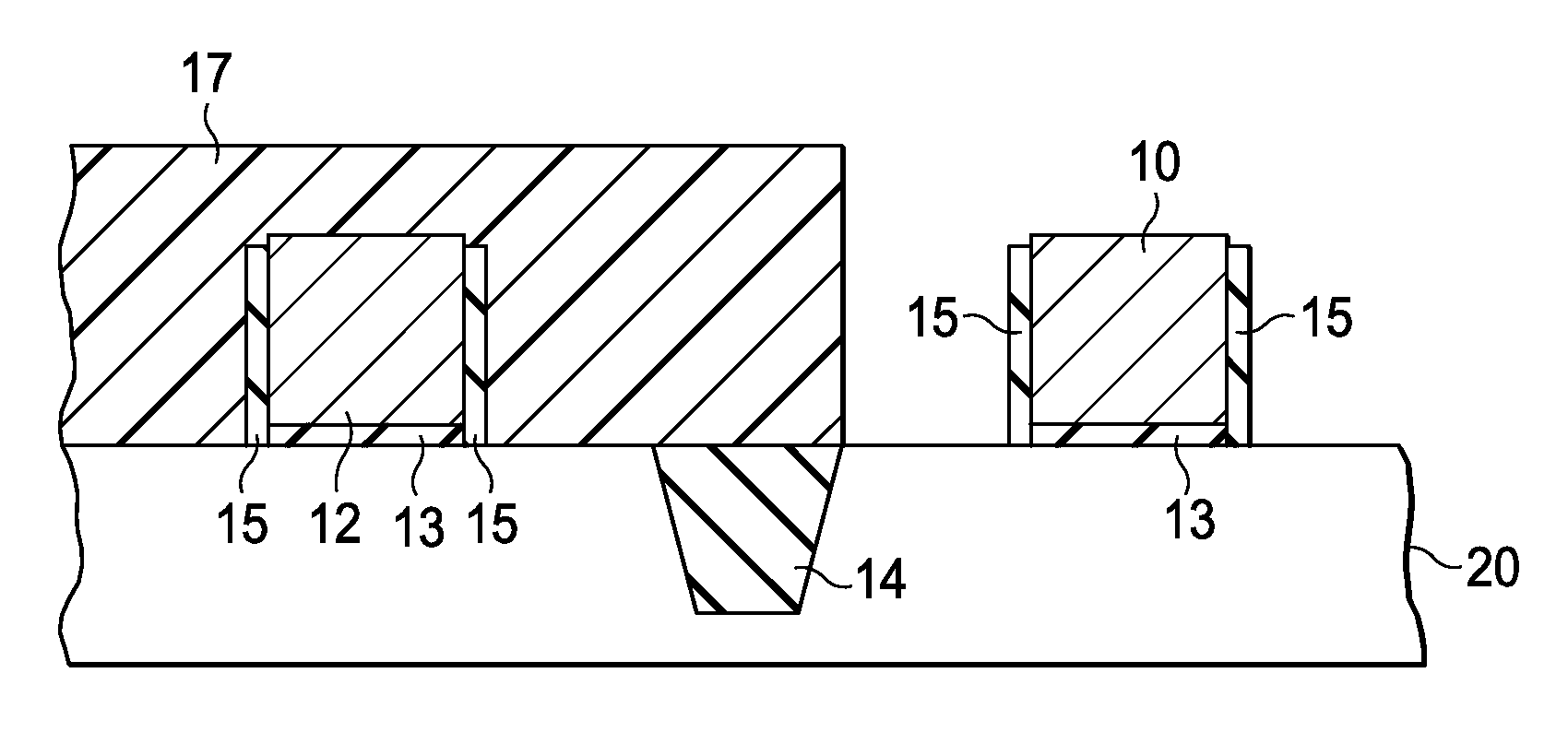
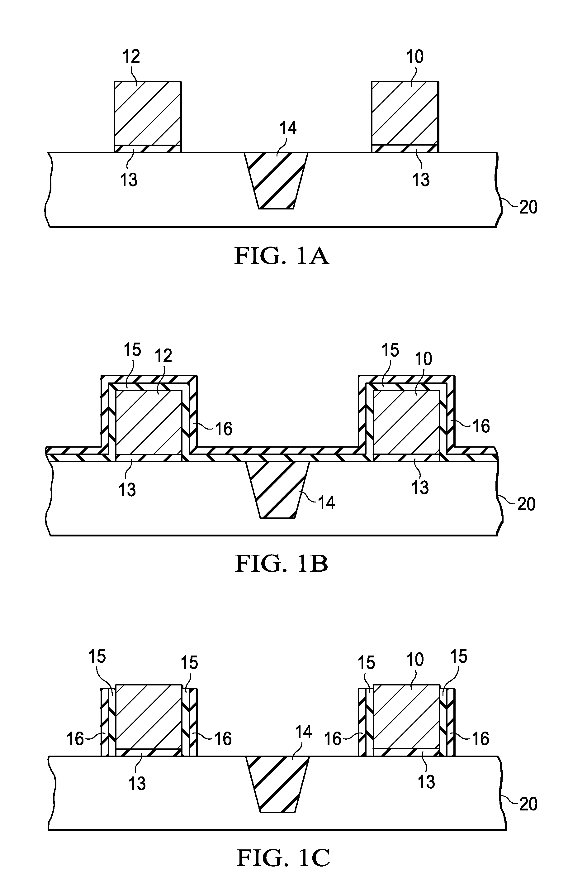
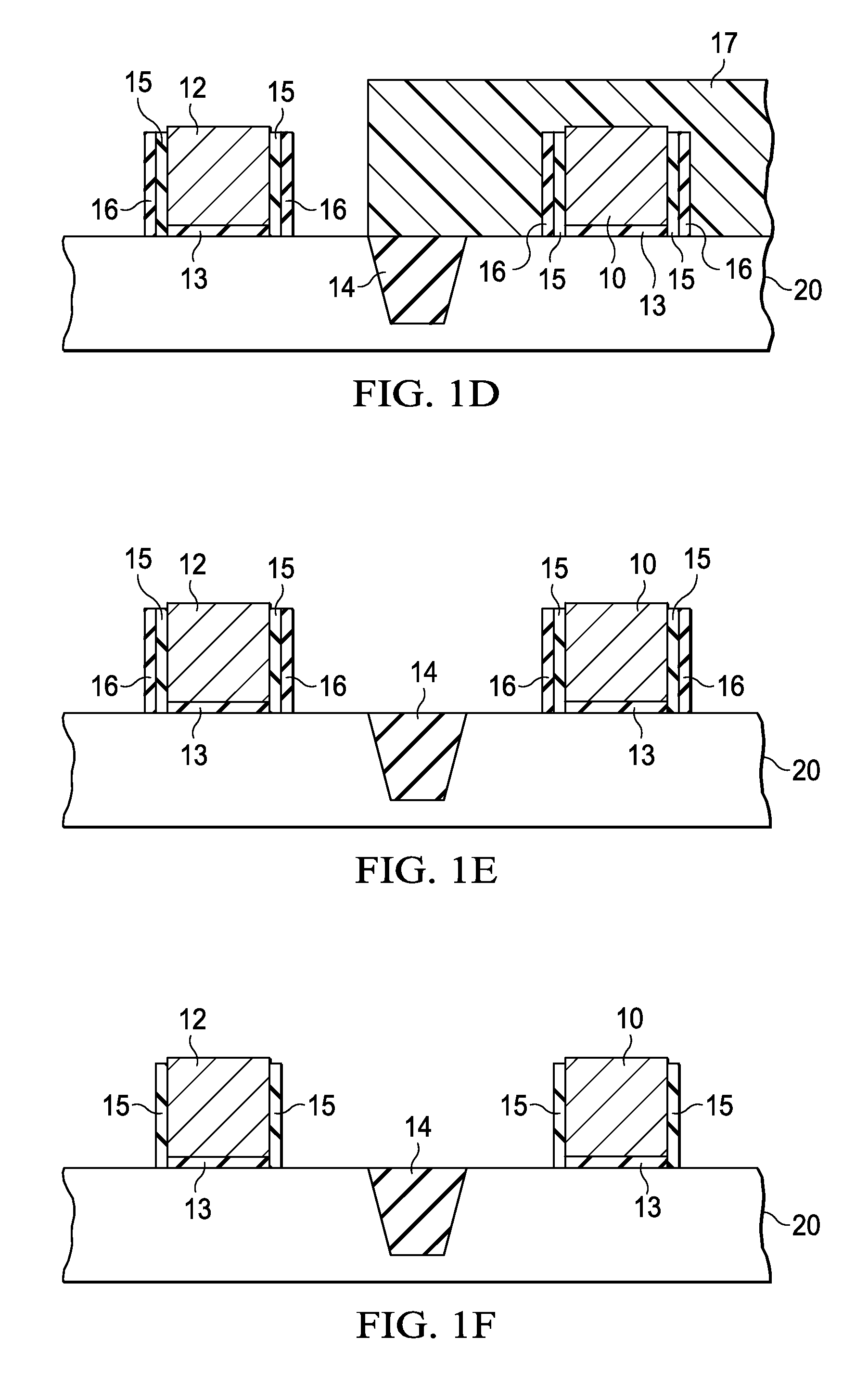
[0015]The present invention will now be described with reference to the attached drawings, wherein like reference numerals are used to refer to like elements throughout. Embodiments of the invention provide differential offset spacers which enable optimizing the offset spacer for transistors based on its application / function or location in the circuit without requiring any extra patterning / masking layers. Thus, in one embodiment of the invention, a portion of both the PMOS and NMOS transistors are processed using a thicker offset spacer and a portion of both the PMOS and NMOS transistors are processed using a thinner offset spacer. The invention is broadly applicable to CMOS integrated circuits.

[0016]FIG. 1A-G shows successive cross sectional views during a process sequence to implement an integrated circuit having differential offset spacers according to an embodiment of the invention. FIG. 1A shows defined polysilicon gates 10 and 12 formed on substrate 20 having a semiconducting ...


PUM


Abstract

A method of fabricating a CMOS integrated circuit includes the steps of providing a substrate having a semiconductor surface, forming a gate dielectric and a plurality of gate electrodes thereon in both NMOS and PMOS regions using the surface. A multi-layer offset spacer stack including a top layer and a compositionally different bottom layer is formed and the multi-layer spacer stack is etched to form offset spacers on sidewalls of the gate electrodes. The transistors designed to utilize a thinner offset spacer are covered with a first masking material, and transistors designed to utilize a thicker offset spacer are patterned and first implanted. At least a portion of the top layer is removed to leave the thinner offset spacers on sidewalls of the gate electrodes. The transistors designed to utilize the thicker offset spacer are covered with a second masking material, and the transistors designed to utilize the thinner offset spacer are patterned and second implanted. The fabrication of the integrated circuit is then completed.

Description

FIELD OF INVENTION[0001]The present invention relates generally to semiconductor processing, and more particularly to CMOS processing flows which utilize differential spacers.BACKGROUND[0002]In a conventional CMOS processes, the same spacer structure generally including a sidewall and optional offset spacer on the gate sidewalls is used to form all transistors in the integrated circuit. Although a single spacer structure simplifies the process flow, a conventional single spacer process does not provide flexibility with respect to the application / function for a given transistor (e.g. high voltage or speed), nor the type of transistor (e.g. PMOS or NMOS).[0003]For example, NMOS and PMOS transistors may require different offset spacer widths for transistor performance optimization. Moreover, depending on application / function of a specific transistor in the circuit, it may provide better performance having a relatively thin or a relatively thick (wider) offset spacer. For example, regar...

Claims


Application Information

Patent Timeline
Patent Type & Authority Patents(United States)
IPC IPC(8): H01L21/8238H01L21/336
CPCG11C11/412H01L21/823864H01L27/11H01L27/1104H10B10/00H10B10/12
Inventor EKBOTE, SHASHANKRILEY, DEBORAH J.OBRADOVIC, BORNA
Owner TEXAS INSTR INC
Why Eureka
Try Eureka