

Standard cell, standard cell library, and semiconductor integrated circuit with suppressed variation in characteristics
a technology characteristics, applied in the direction of semiconductor devices, electrical devices, transistors, etc., can solve the problems of affecting the characteristics of transistors severely, the final dimension variation of various patterns, and the lowering of yield and reliability of semiconductor integrated circuits. , to achieve the effect of suppressing the variation in characteristics of a standard cell
- Summary
- Abstract
- Description
- Claims
- Application Information
AI Technical Summary
Benefits of technology
Problems solved by technology
Method used
Image

Examples
first embodiment
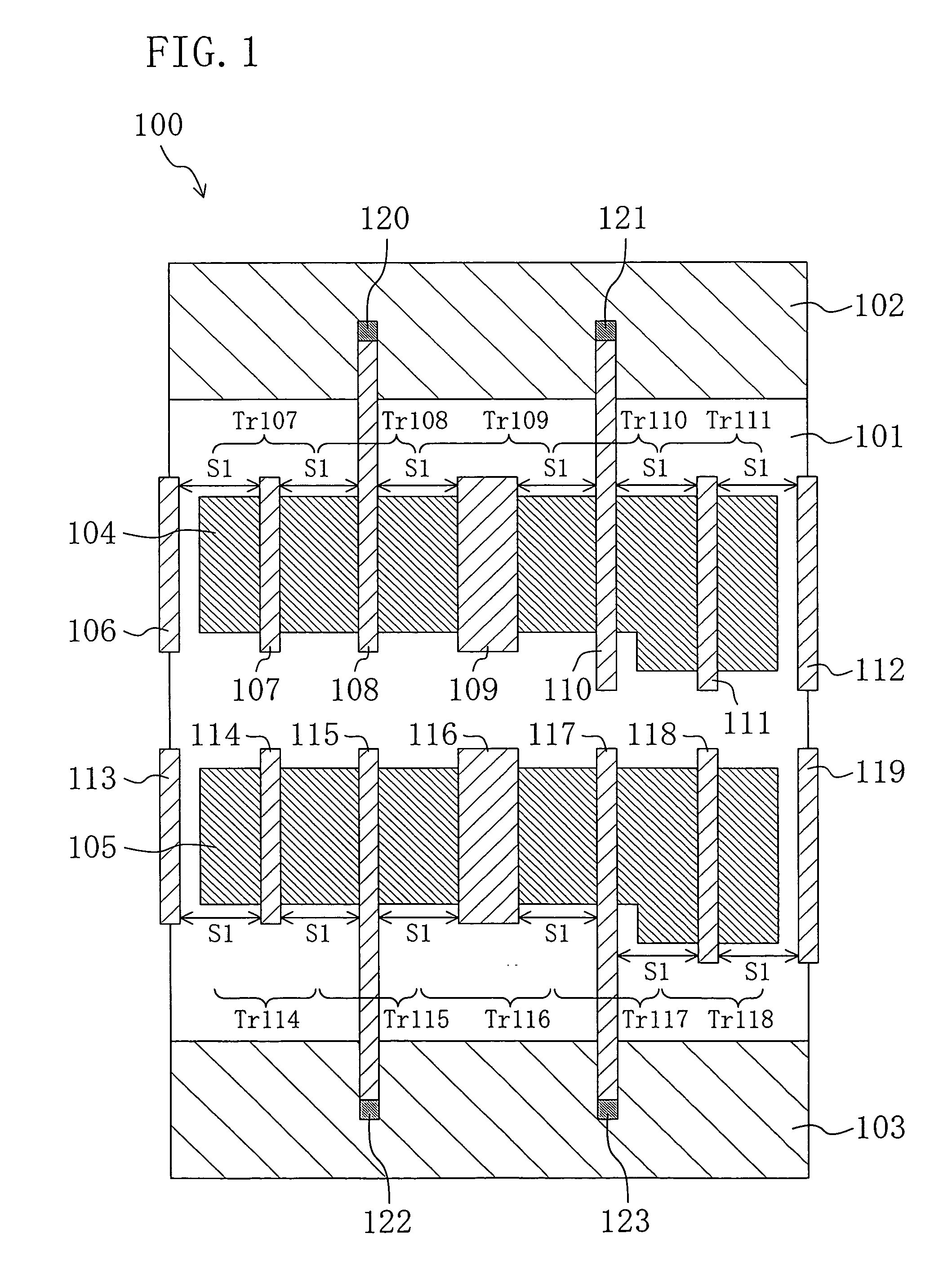
[0076]FIG. 1 is a plan view showing a standard cell according to the first embodiment of the present invention. As shown in FIG. 1, a standard cell 100 of the present embodiment includes: a semiconductor layer 101; a source wiring 102 provided at one end of the semiconductor layer 101; a ground wiring 103 provided at one end opposite the source wiring 102 of the semiconductor layer 101; a p-type diffusion region 104 provided in a region located between the source wiring 102 and the ground wiring 103 in the semiconductor layer 101; a n-type diffusion region 105 provided in a region other than the p-type diffusion region 104 in the semiconductor layer 101; gates 107 to 111 provided on the p-type diffusion region 104 at a spacing S1 from each other; gates 114 to 118 provided on the n-type diffusion region 105 at the spacing S1 from each other; dummy gates 106, 112 provided on both the sides of the p-type diffusion region 104 in the semiconductor layer 101 with the spacing S1 from the g...
second embodiment
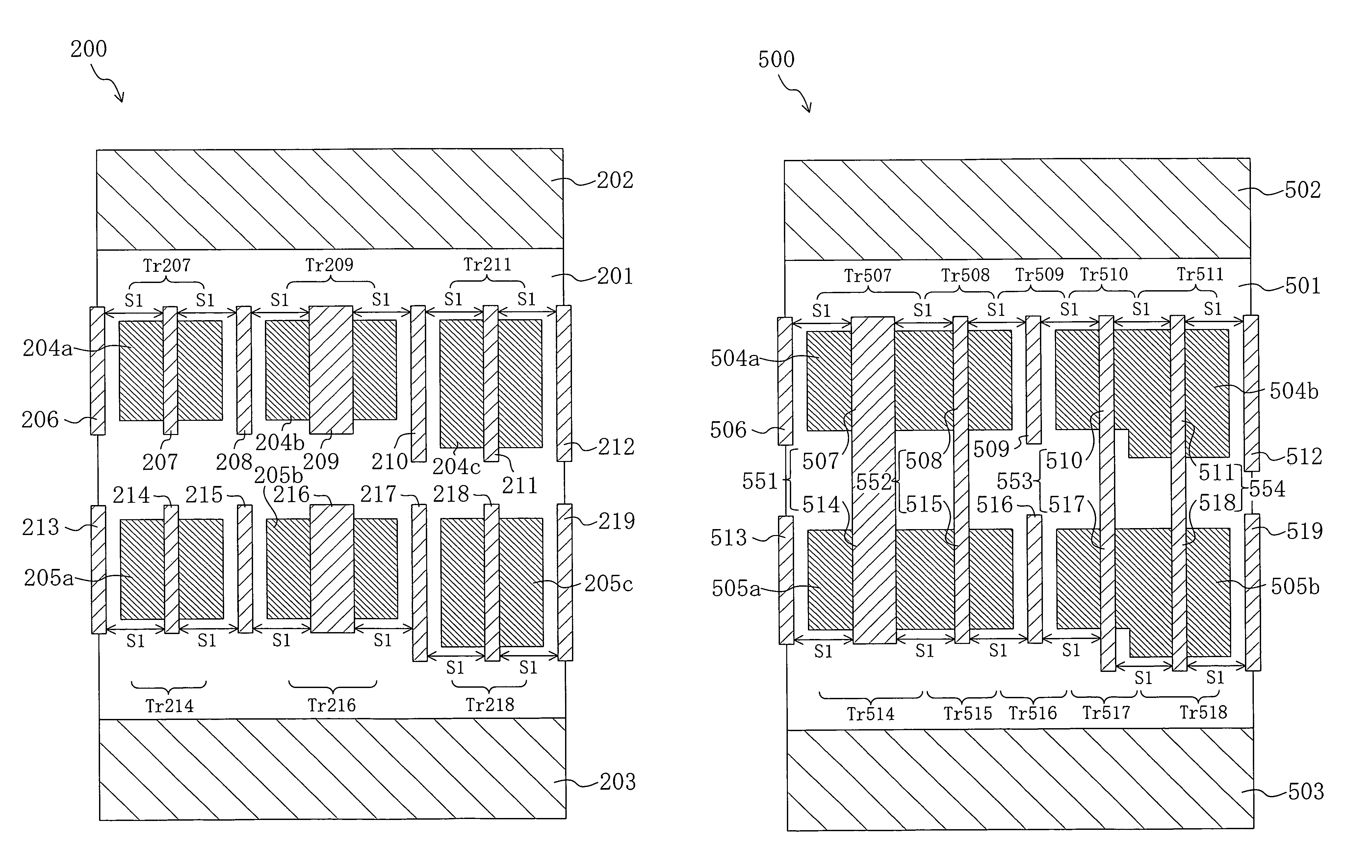
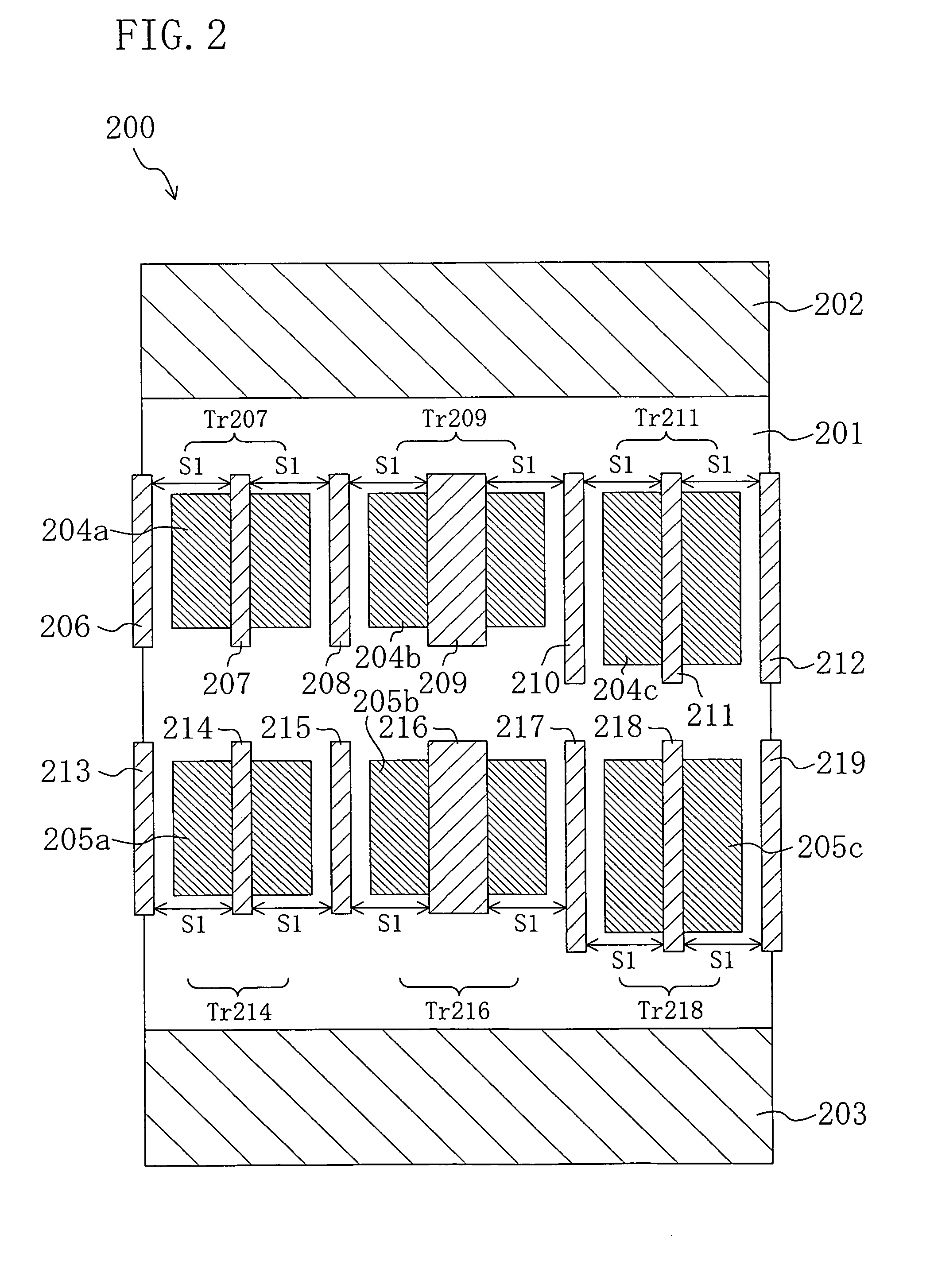
[0084]FIG. 2 is a plan view showing a standard cell of a second embodiment of the present invention. As shown in FIG. 2. a standard cell 200 of the present embodiment includes: a semiconductor layer 201; a source wiring 202 provided at one end of the semiconductor layer 201; a ground wiring 203 provided at one end opposite the source wiring 202 of the semiconductor layer 201; p-type diffusion regions 204a, 204b, 204c provided in regions located between the source wiring 202 and the ground wiring 203 in the semiconductor layer 201, respectively; n-type diffusion regions 205a, 205b, 205c provided in regions other than the p-type diffusion regions 204a, 204b, 204c in the semiconductor layer 201, respectively; gates 207, 209, 211 provided on the p-type diffusion regions 204a, 204b, 204c, respectively; gates 214, 216, 218 provided on the n-type diffusion regions 205a, 205b, 205c, respectively; dummy gates 206, 208, 210, 212 provided between or on one side of the p-type diffusion regions ...
third embodiment
[0091]FIG. 3 is a plan view of a standard cell according to a third embodiment of the present invention. As shown in FIG. 3, a standard cell 300 of the present embodiment includes: a semiconductor layer 301; a source wiring 302 provided at one end of the semiconductor layer 301; a ground wiring 303 provided at one end opposite the source wiring 302 of the semiconductor layer 301; a p-type diffusion region 304 provided in a region located between the source wiring 202 and the ground wiring 303 in the semiconductor layer 301; a n-type diffusion region 305 provided in a region other than the p-type diffusion region 304 in the semiconductor layer 301; gates 307 to 311 provided apart from each other on the p-type diffusion region 304; gates 314 to 318 provided apart from each other on the n-type diffusion region 305; dummy gates 306, 312 provided on parts on the sides of the p-type diffusion region 304 in the semiconductor layer 301 with a spacing S1 from the gates 307, 311, respectively...
PUM
 Abstract
Description
Claims
Application Information