Silicon carbide ingot and silicon carbide substrate, and method of manufacturing the same

a technology of silicon carbide and ingot, which is applied in the direction of polycrystalline material growth, transportation and packaging, after-treatment details, etc., can solve the problems of not particularly adjusting the arrangement or the size of the (0001) facet plane, and achieve excellent uniformity and low yield of the device formed on the silicon carbide substra

Inactive Publication Date: 2013-04-18
SUMITOMO ELECTRIC IND LTD
View PDF4 Cites 11 Cited by
  • Summary
  • Abstract
  • Description
  • Claims
  • Application Information

AI Technical Summary

Benefits of technology

[0023]In the silicon carbide substrate according to this invention, an area of a circumcircle surrounding the entire pattern present on one main surface above and coming in contact with an outermost portion of at least one pattern is not more than 90% of an area of the entire one main surface above. When the area of the circumcircle above exceeds 90% of the area of the entire one main surface, the patterns are scattered on substant

Problems solved by technology

In a silicon carbide ingot formed with a conventional method, however, arrangement or a size of the (0001) facet

Method used


Image

  • Silicon carbide ingot and silicon carbide substrate, and method of manufacturing the same
  • Silicon carbide ingot and silicon carbide substrate, and method of manufacturing the same
  • Silicon carbide ingot and silicon carbide substrate, and method of manufacturing the same

Examples


example

[0142]In order to confirm an effect of the present invention, an ingot and a substrate were manufactured and characteristics were measured with a method as below.

Sample

[0143]Samples in Examples and Comparative Examples according to the present invention, of a silicon carbide ingot and a silicon carbide substrate obtained by slicing the silicon carbide ingot, were prepared as below.

Base Substrate for Sample in Example According to the Present Invention

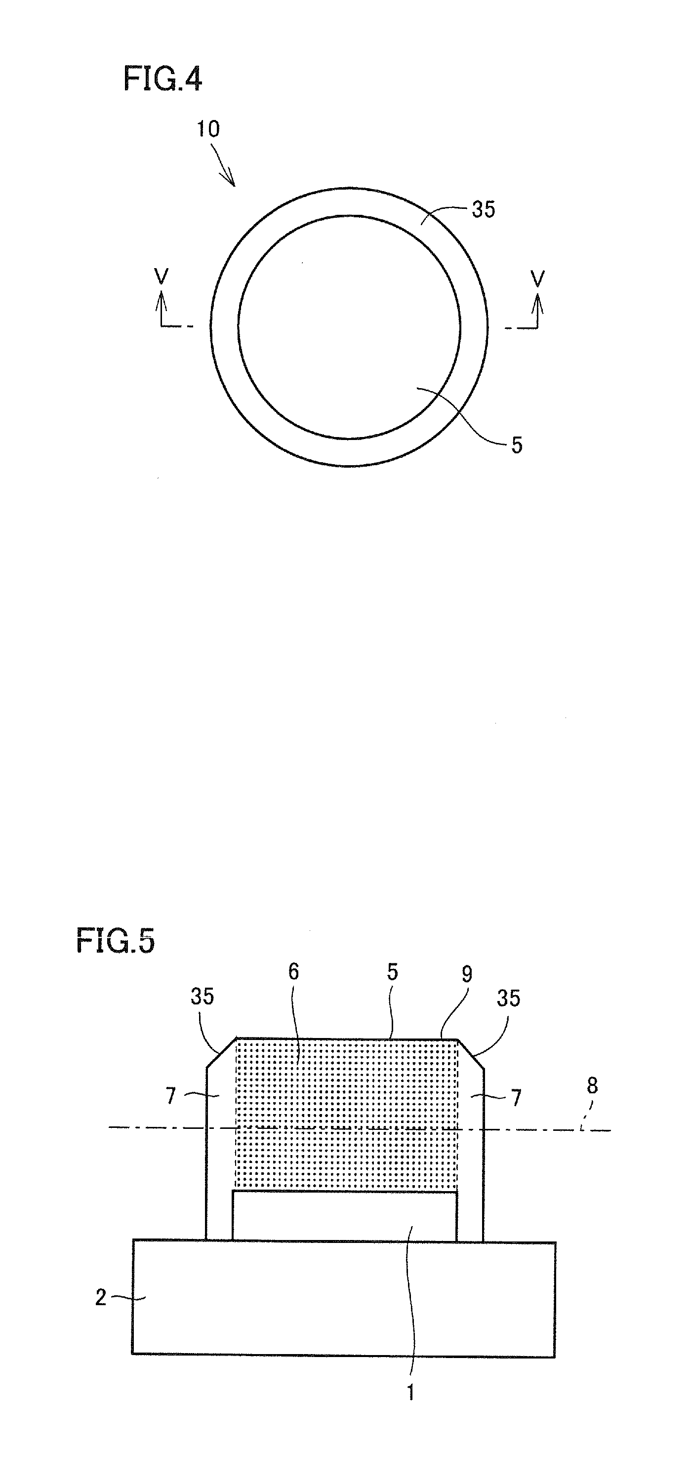
[0144]In order to manufacture a silicon carbide ingot, a silicon carbide single crystal substrate satisfying conditions as below was prepared as a base substrate. Specifically, in order to manufacture an ingot according to the present invention, 3 SiC single crystal substrates of 4H type were prepared as base substrates 1. Base substrate 1 can have a range of a diameter from 50 to 180 mm and a range of thickness from 100 to 2000 μm. Here, a thickness of base substrate 1 was set to 800 μm. In addition, an off angle of the main surface of...

experiment method

Manufacturing of Ingot

Ingot According to Example

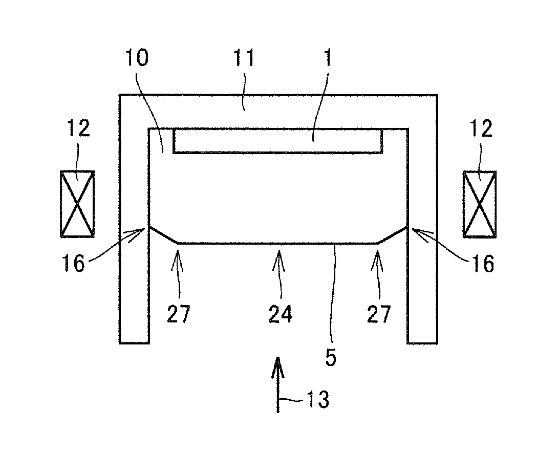
[0146]A silicon carbide epitaxial layer was formed on the surface of the base substrate for Example described above, to thereby manufacture a silicon carbide ingot according to Example. Specifically, base substrate 1 and powdery SiC serving as a source material were introduced in a crucible made of graphite. A distance between the source material and the base substrate was set in a range from 10 mm to 100 mm. With regard to a growth method, manufacturing is carried out generally with a method called a sublimation method or an improved Raleigh method. Specifically, this crucible was set in the inside of a heating furnace and a temperature was increased. During temperature increase, a pressure of an atmosphere was set in a range from 50 kPa to an atmospheric pressure. A temperature during crystal growth was set such that a temperature in a lower portion of the crucible was not lower than 2200° C. and not higher than 2500° C. and a temper...


PUM

PropertyMeasurementUnit
Fractionaaaaaaaaaa
Fractionaaaaaaaaaa
Thicknessaaaaaaaaaa

Abstract

A silicon carbide ingot excellent in uniformity in characteristics and a silicon carbide substrate obtained by slicing the silicon carbide ingot, and a method of manufacturing the same are obtained. A method of manufacturing a silicon carbide ingot includes the steps of preparing a base substrate having an off angle with respect to a (0001) plane not greater than 1° and composed of single crystal silicon carbide and growing a silicon carbide layer on a surface of the base substrate. In the step of growing a silicon carbide layer, a temperature gradient in a direction of width when viewed in a direction of growth of the silicon carbide layer is set to 10° C./cm or less.

Description

BACKGROUND OF THE INVENTION[0001]1. Field of the Invention[0002]This invention relates to a silicon carbide ingot and a silicon carbide substrate, and a method of manufacturing the same, and more particularly to a silicon carbide ingot less in variation in such characteristics as impurity concentration and a silicon carbide substrate obtained by slicing the silicon carbide ingot, and a method of manufacturing the same.[0003]2. Description of the Background Art[0004]Silicon carbide (SiC) has conventionally been studied as a next-generation semiconductor material replacing silicon (Si). In order to manufacture a substrate composed of this silicon carbide, a method of manufacturing a substrate by growing a silicon carbide single crystal on a seed substrate to form a silicon carbide ingot and slicing the silicon carbide ingot has conventionally been known. In this case, a method of preparing a seed crystal with a (0001) plane (what is called a c plane) or a crystal plane having an off a...

Claims


Application Information

Patent Timeline
IPC IPC(8): C30B23/02C30B29/68C30B33/00C30B29/36
CPCC30B23/025C30B29/36C30B29/68Y10T29/49995Y10T428/24488Y10T428/24479C30B33/00
Inventor SASAKI, MAKOTOHARADA, SHINNISHIGUCHI, TARO
Owner SUMITOMO ELECTRIC IND LTD
Why Eureka
Try Eureka