Layout method and layout apparatus for semiconductor integrated circuit

a technology for integrated circuits and layout methods, applied in cad circuit design, computer aided design, instruments, etc., can solve problems such as deterioration of product performance, product performance degradation, and yield declin

Inactive Publication Date: 2009-04-09
RENESAS ELECTRONICS CORP
View PDF5 Cites 13 Cited by
  • Summary
  • Abstract
  • Description
  • Claims
  • Application Information

AI Technical Summary

Benefits of technology

[0017]In a layout method and a layout apparatus for a semiconductor integrated circuit according to the present invention, a variation in characteristics of a transistor in a semiconductor integrated circuit, which is caused based on a data density of gates, can be suppressed.

Problems solved by technology

However, with reduction in a wiring width in the LSI, variation in a gate size due to an optical proximity effect and variation in an amount of etching causes a problem.
Variation in characteristics of a transistor due to variation in gate size degrades product performance and contributes to a decrease in yields.
For this reason, according to the layout method of the conventional technique, driving characteristics of a transistor provided in the vicinity of the boundary of adjacent cells in the column direction are within a variation, deteriorating product performance.

Method used


Image

  • Layout method and layout apparatus for semiconductor integrated circuit
  • Layout method and layout apparatus for semiconductor integrated circuit
  • Layout method and layout apparatus for semiconductor integrated circuit

Examples


first embodiment

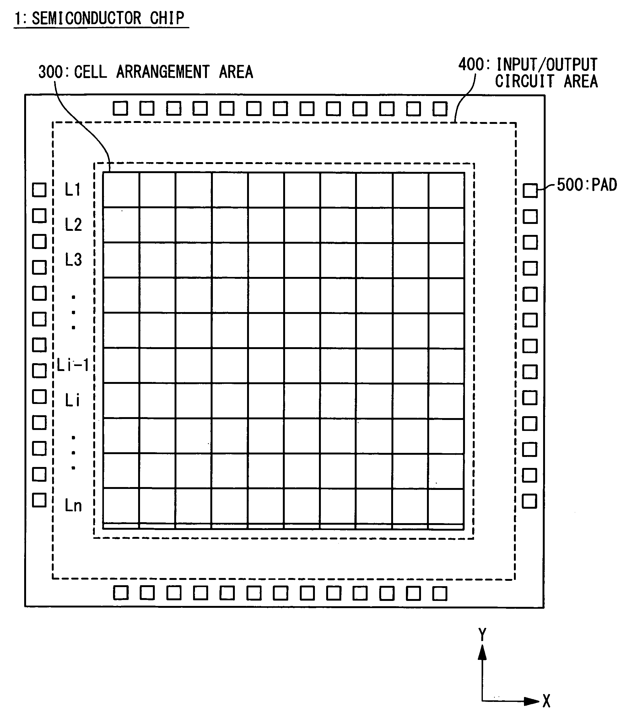
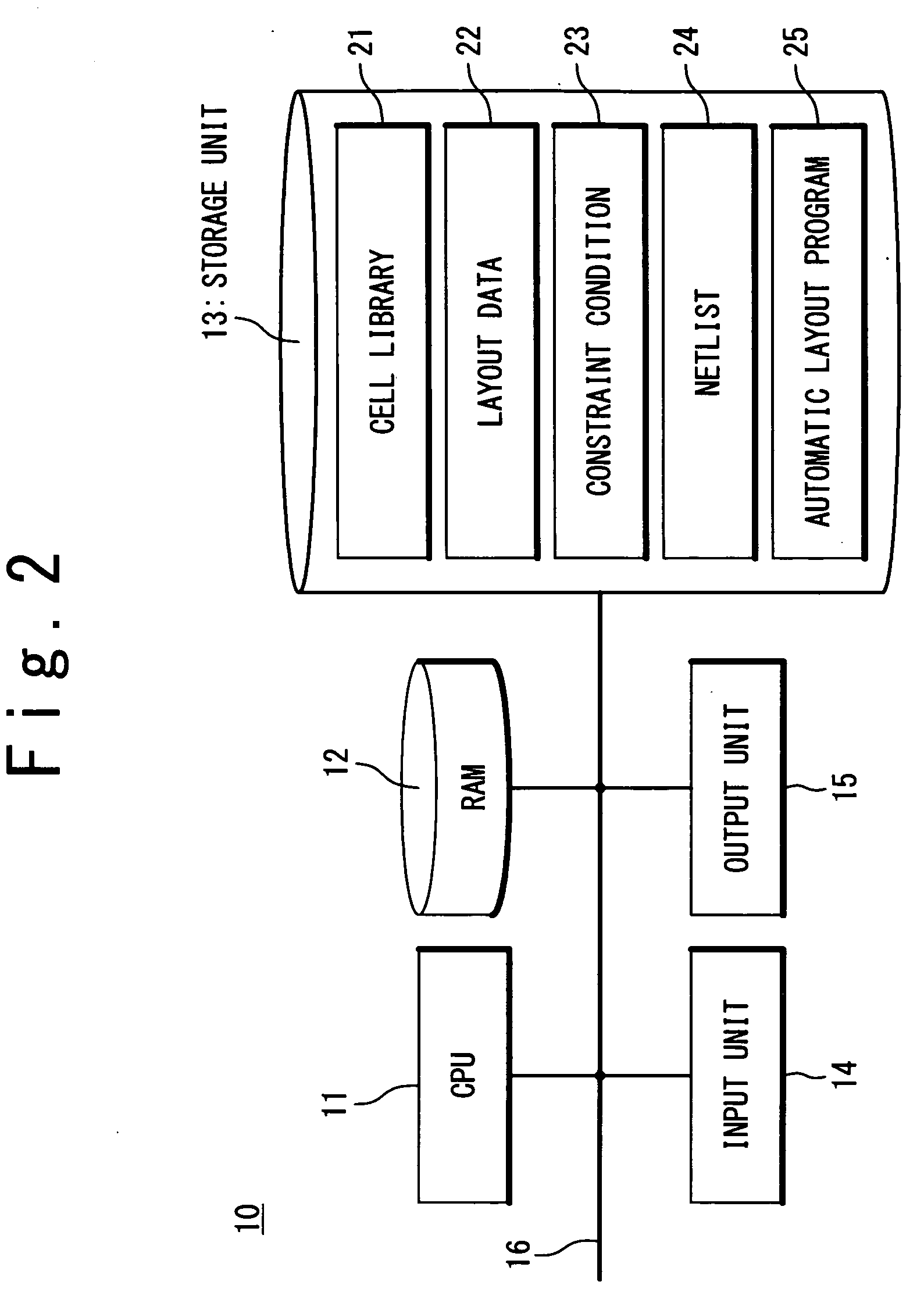
[0034]Referring to FIGS. 2 and 3, a configuration of an automatic layout apparatus 10 for a semiconductor integrated circuit according to a first embodiment of the present invention will be described. FIG. 2 is a block diagram showing the configuration of the automatic layout apparatus 10 according to the first embodiment of the present invention. The automatic layout apparatus 10 includes a CPU 11, a RAM 12, a storage unit 13, an input unit 14 and an output unit 15 which are interconnected via a bus 16. The storage unit 13 is an external storage unit such as a hard disc or a memory unit. The input unit 14 is operated by a user by using a keyboard, a mouse or the like to input various data. The output unit 15 is exemplified to a monitor or a printer and visually represents a semiconductor layout outputted from the CPU 11 to the user.

[0035]The storage unit 13 stores a cell library 21 for automatic layout, layout data 22, a constraint condition 23, a netlist 24 and an automatic layout...

second embodiment

[0066]Referring to FIG. 14, a configuration and an operation of a layout apparatus 10 according to a second embodiment of the present invention will be described. The layout apparatus 10 in the second embodiment does not extracts the layout coordinates of the effective gate patterns 102 from the corrected library data 212, but extracts the layout coordinates of the effective gate patterns 102 by referring to the layout data 22, unlike the layout apparatus 10 in the first embodiment.

[0067]Hereinafter, the same reference numerals are assigned to same components as those in the first embodiment. Description of the similar configuration and operations to those in the first embodiment is omitted and only differences will be described.

[0068]FIG. 14 is a block diagram showing the configuration of the layout apparatus 10 according to the second embodiment of the present invention. The storage unit 13 in the second embodiment stores the library data 211 as the cell library 21. The storage un...


PUM


Abstract

In a layout method for a semiconductor integrated circuit by using cell library data, a plurality of cell patterns are arranged in a first direction. One of gate patterns in one of the plurality of cell patterns is specified as a reference gate pattern. An additional cell pattern is arranged in a second direction orthogonal to the first direction such that a number of gate patterns within a predetermined area containing the reference gate pattern satisfies a constraint condition.

Description

INCORPORATION BY REFERENCE[0001]This patent application claims priority on convention based on Japanese Patent Application No. 2007-233285 filed on Sep. 7, 2007. The disclosure thereof is incorporated herein by reference.BACKGROUND OF THE INVENTION[0002]1. Field of the Invention[0003]The present invention relates to a layout method and a layout apparatus for a semiconductor integrated circuit, and more particularly, to a layout method, and a layout apparatus for a semiconductor integrated circuit for performing cell-based layout of a semiconductor integrated circuit by using library data.[0004]2. Description of Related Art[0005]A cell-based IC (Integrated Circuit) is suitably used for an LSI such as an ASIC (Application Specific Integrated Circuit), an ASSP (Application Specific Standard Product) and a microprocessor, in which high integration and high performance are requested. The cell-based IC is manufactured by combining cells provided by a semiconductor maker and individual cir...

Claims


Application Information

Patent Timeline
Patent Type & Authority Applications(United States)
IPC IPC(8): H01L21/77H01L21/98
CPCH01L27/11807G06F17/5068G06F30/39
Inventor KOBAYASHI, NAOHIRO
Owner RENESAS ELECTRONICS CORP
Why Eureka
Try Eureka