Memory device, semiconductor storage device, method for manufacturing memory device, and reading method for semiconductor storage device

a memory device and semiconductor technology, applied in semiconductor devices, digital storage, instruments, etc., can solve problems such as cross-point reram, and achieve the effects of reducing variation in characteristics of memory devices, substantially miniaturizing memory devices, and greatly improving the embeddability of variable resistance layers in memory devices in which memory cell holes are embedded

Inactive Publication Date: 2013-05-16
PANASONIC SEMICON SOLUTIONS CO LTD
View PDF3 Cites 15 Cited by
  • Summary
  • Abstract
  • Description
  • Claims
  • Application Information

AI Technical Summary

Benefits of technology

[0042]Furthermore, processing dimensions of the variable resistance layer and the diode can be larger than the minimum design dimension of the memory device. Accordingly, the memory device can substantially be miniaturized without using special micromachining process technology. Since the embeddability of the variable resistance layer in the memory device in which the memory cell hole is embedded can be greatly improved, the variation in characteristics of the memory devices can be reduced.
[0043]Furthermore, since variable resistance elements identical in number to the first electrodes can be included in the memory device according to the present invention, the element area of one memory device closer to the diode can be larger than that of the diode closer to the variable resistance element. Accordingly, it is possible to prevent the diode from degrading in the characteristics and being destroyed, due to the current that flows through the diode during an initial break operation and a resistance change operation of the variable resistance element.

Problems solved by technology

However, the cross-point ReRAM has a problem in the influence of variable resistance layers in other rows and columns when a resistance value of a variable resistance layer formed at a cross-point at which the upper electrode and the lower electrode cross is read.

Method used


Image

  • Memory device, semiconductor storage device, method for manufacturing memory device, and reading method for semiconductor storage device
  • Memory device, semiconductor storage device, method for manufacturing memory device, and reading method for semiconductor storage device
  • Memory device, semiconductor storage device, method for manufacturing memory device, and reading method for semiconductor storage device

Examples


embodiment 1

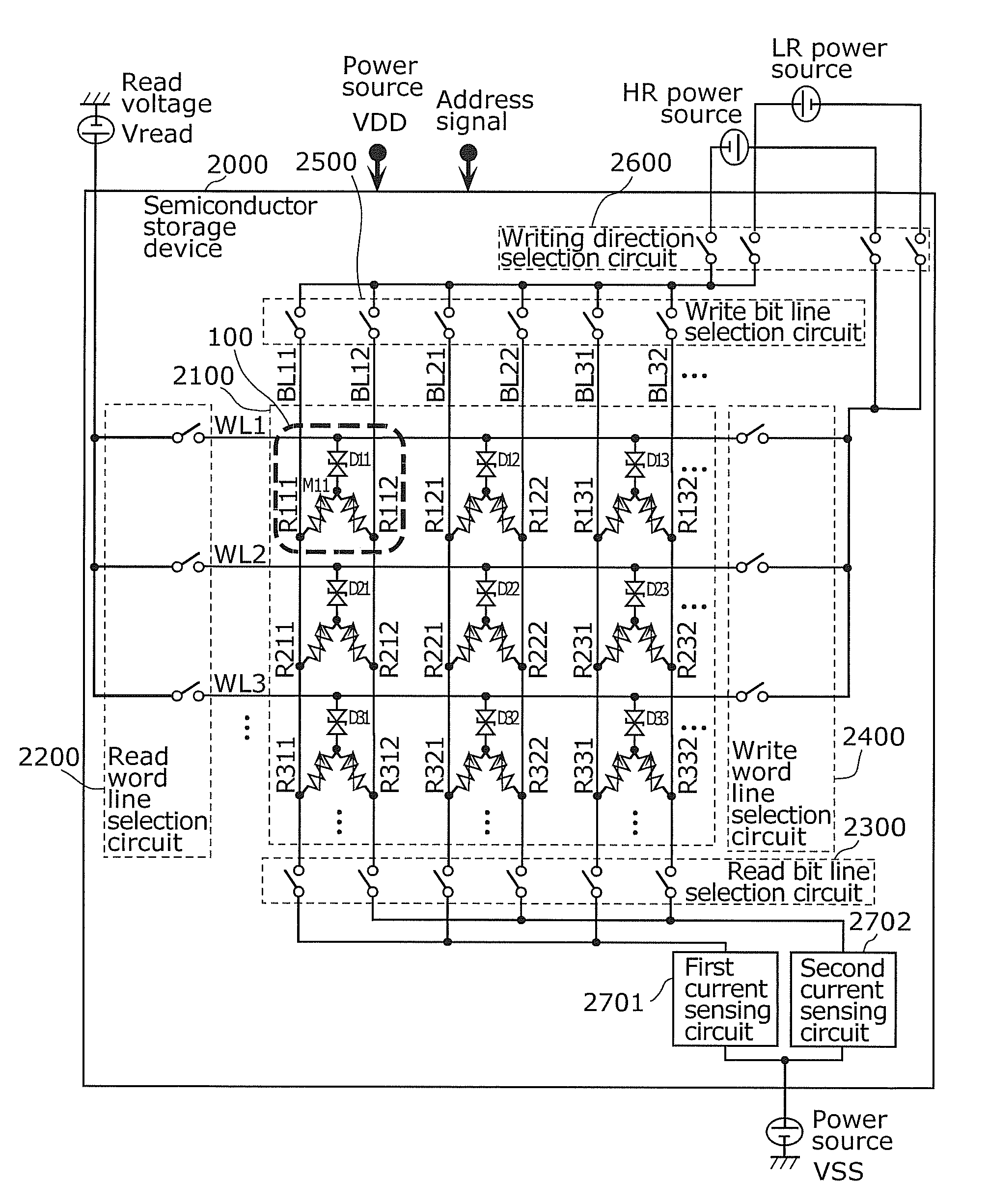
[0133]Hereinafter, a memory device, a method for manufacturing a memory device, a semiconductor storage device, and writing and read operations by the semiconductor storage device according to Embodiment 1 of the present invention will be described with reference to the drawings.

[0134][Structure of Memory Device]

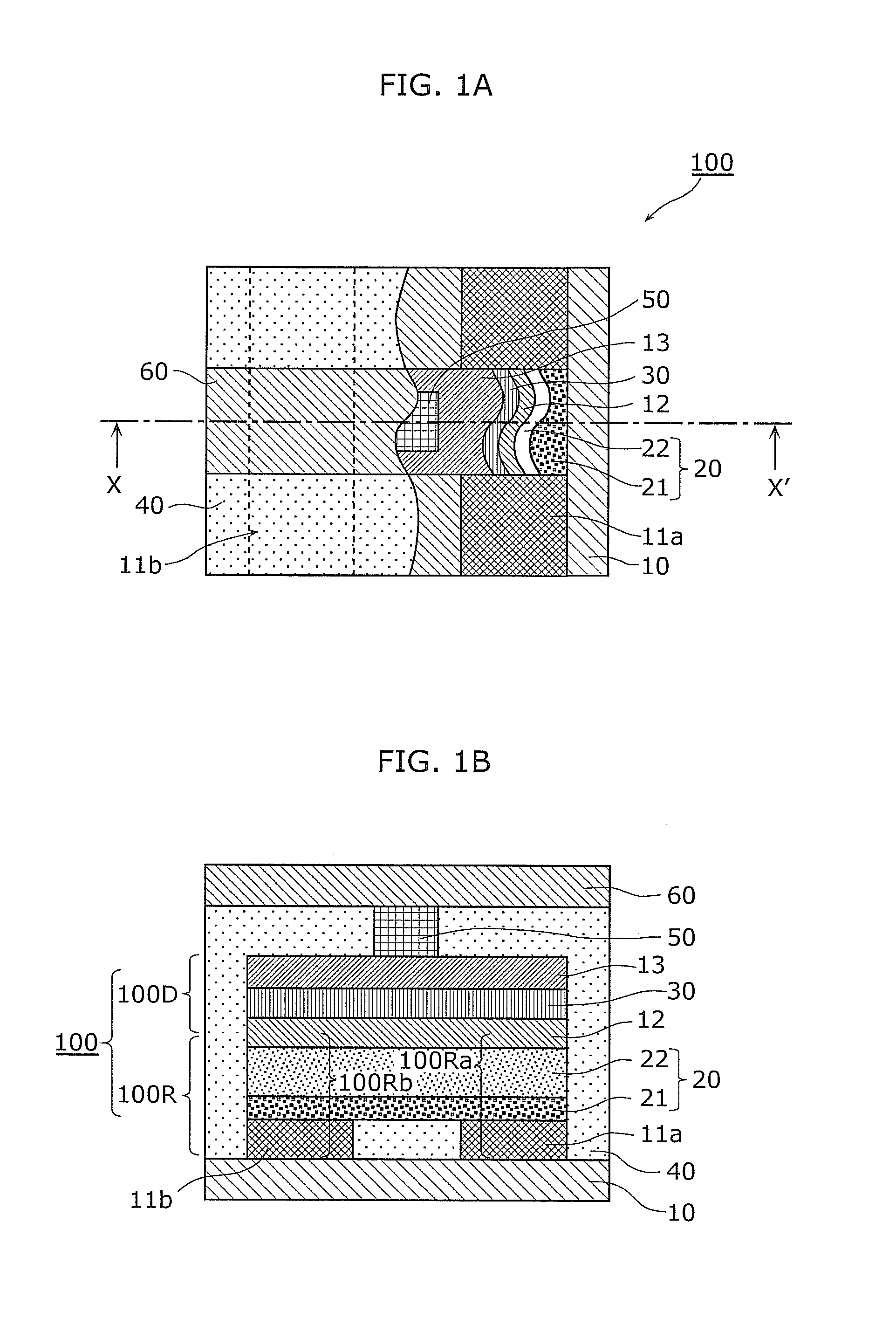
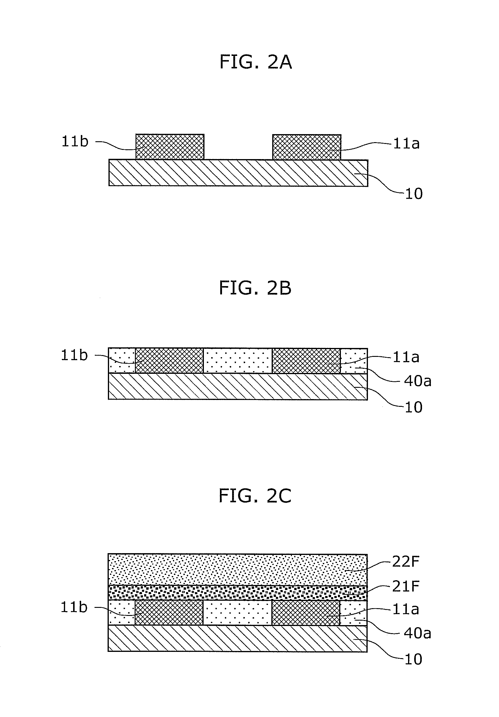
[0135]A memory device 100 according to Embodiment 1 will be described with reference to FIGS. 1A and 1B. FIG. 1A is a partially cutout plan view illustrating a structure of a memory device according to Embodiment 1. Furthermore, FIG. 1B is a section view illustrating the structure of the memory device cut along an X-X′ line in FIG. 1A.

[0136]As illustrated in FIGS. 1A and 1B, the memory device 100 according to Embodiment 1 is a planar memory device, and includes two first electrodes 11a and 11b, a second electrode 12, a third electrode 13, a variable resistance layer 20 between the first electrodes 11a and 11b and the second electrode 12, and a non-conductive layer 30 between...

embodiment 2

[0236]Next, a memory device and a method for manufacturing the memory device according to Embodiment 2 will be described with reference to the drawings. A semiconductor storage device and a write operation and a read operation performed by the semiconductor storage device according to Embodiment 2 are the same as those according to Embodiment 1, and thus, the description thereof is omitted.

[0237][Structure of Memory Device]

[0238]A memory device 200 according to Embodiment 2 will be described with reference to FIGS. 9A and 9B. FIG. 9A is a partially cutout plan view illustrating a structure of a memory device according to Embodiment 2. Furthermore, FIG. 9B is a section view illustrating the structure of the memory device cut along an X-X′ line in FIG. 9A. Embodiment 2 will be described using two variable resistance elements formed in a single memory device as an example, as according to Embodiment 1.

[0239]The memory device 200 in FIGS. 9A and 9B according to Embodiment 2 has the same...

embodiment 3

[0257]Next, a memory device and a method for manufacturing the memory device according to Embodiment 3 will be described with reference to the drawings. A semiconductor storage device and a write operation and a read operation performed by the semiconductor storage device according to Embodiment 3 are the same as those according to Embodiment 1, and thus, the description thereof is omitted.

[0258][Structure of Memory Device]

[0259]First, a memory device 300 according to Embodiment 3 will be described with reference to FIGS. 11A and 11B. FIG. 11A is a partially cutout plan view illustrating a structure of the memory device according to Embodiment 3. Furthermore, FIG. 11B is a section view illustrating the structure of the memory device cut along an X-X′ line in FIG. 11A. Embodiment 3 will be described using two variable resistance elements formed in a single memory device as an example, as according to Embodiments 1 and 2.

[0260]The memory device 300 in FIGS. 11A and 11B according to Em...


PUM


Abstract

A memory device that can prevent degradation in characteristics of a diode and the destruction due to the miniaturization includes: a substrate; first electrodes, a second electrode, and a third electrode that are stacked above the substrate; a variable resistance layer between the first and second electrodes; and a non-conductive layer between the second and third electrodes. The variable resistance layer includes a high-concentration variable resistance layer closer to the first electrodes, and a low-concentration variable resistance layer closer to the second electrode and having an oxygen concentration lower than that of the high-concentration variable resistance layer. The second and third electrodes and the non-conductive layer comprise the diode, and the first and second electrodes and the variable resistance layer comprise variable resistance elements, a total number of which is equal to that of the first electrodes.

Description

TECHNICAL FIELD[0001]The present invention relates to a memory device, a semiconductor storage device, a method for manufacturing a memory device, and a reading method for a semiconductor storage device. The present invention relates particularly to a memory device including a variable resistance element connected in series with a diode, a cross-point nonvolatile semiconductor storage device including the memory device, a method for manufacturing the memory device, and a reading method for the cross-point nonvolatile semiconductor storage device.BACKGROUND ART[0002]Recent years have seen increasingly higher performance in electronic devices such as portable information devices and information appliances, following the development of digital technology. As such, there is an increased demand for increasing capacity, reducing writing power consumption, accelerating speed during writing and reading, and extending operational life, in nonvolatile semiconductor memory devices.[0003]In vie...

Claims


Application Information

Patent Timeline
Patent Type & Authority Applications(United States)
IPC IPC(8): H01L45/00G11C13/00
CPCH01L27/101G11C2213/78H01L45/08H01L45/1233H01L45/146H01L45/1675H01L45/1683H01L27/2472G11C13/004H01L45/1253H01L45/16H01L27/2409H01L45/1625G11C13/003G11C13/0069G11C2013/0073G11C2213/72G11C13/0007H10B63/82H10B63/20H10N70/24H10N70/826H10N70/8833H10N70/026H10N70/066H10N70/063H10N70/841H10N70/011
Inventor TSUJI, KIYOTAKAMIKAWA, TAKUMI
Owner PANASONIC SEMICON SOLUTIONS CO LTD
Why Eureka
Try Eureka