

Photolithographic systems and methods for producing sub-diffraction-limited features
a technology of photolithography and features, applied in the field of photolithography systems and methods, can solve the problems of complex lenses, incompatibility of fluid and wafer, high cost,
- Summary
- Abstract
- Description
- Claims
- Application Information
AI Technical Summary
Benefits of technology
Problems solved by technology
Method used
Image

Examples
Embodiment Construction
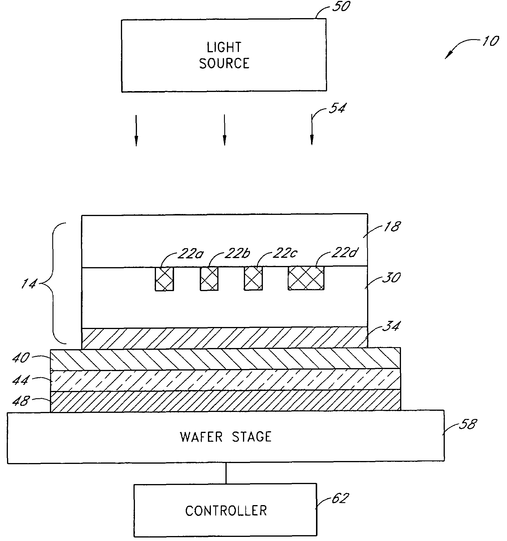
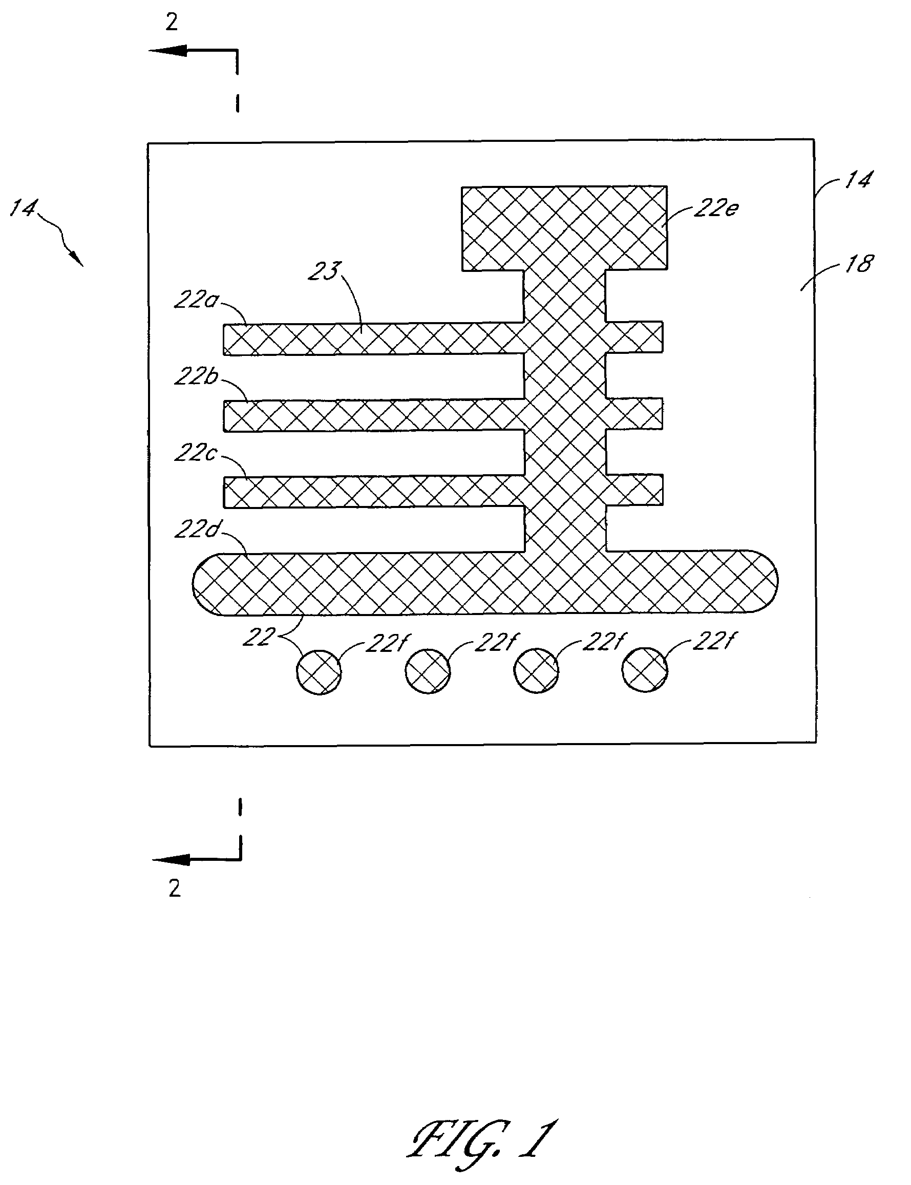
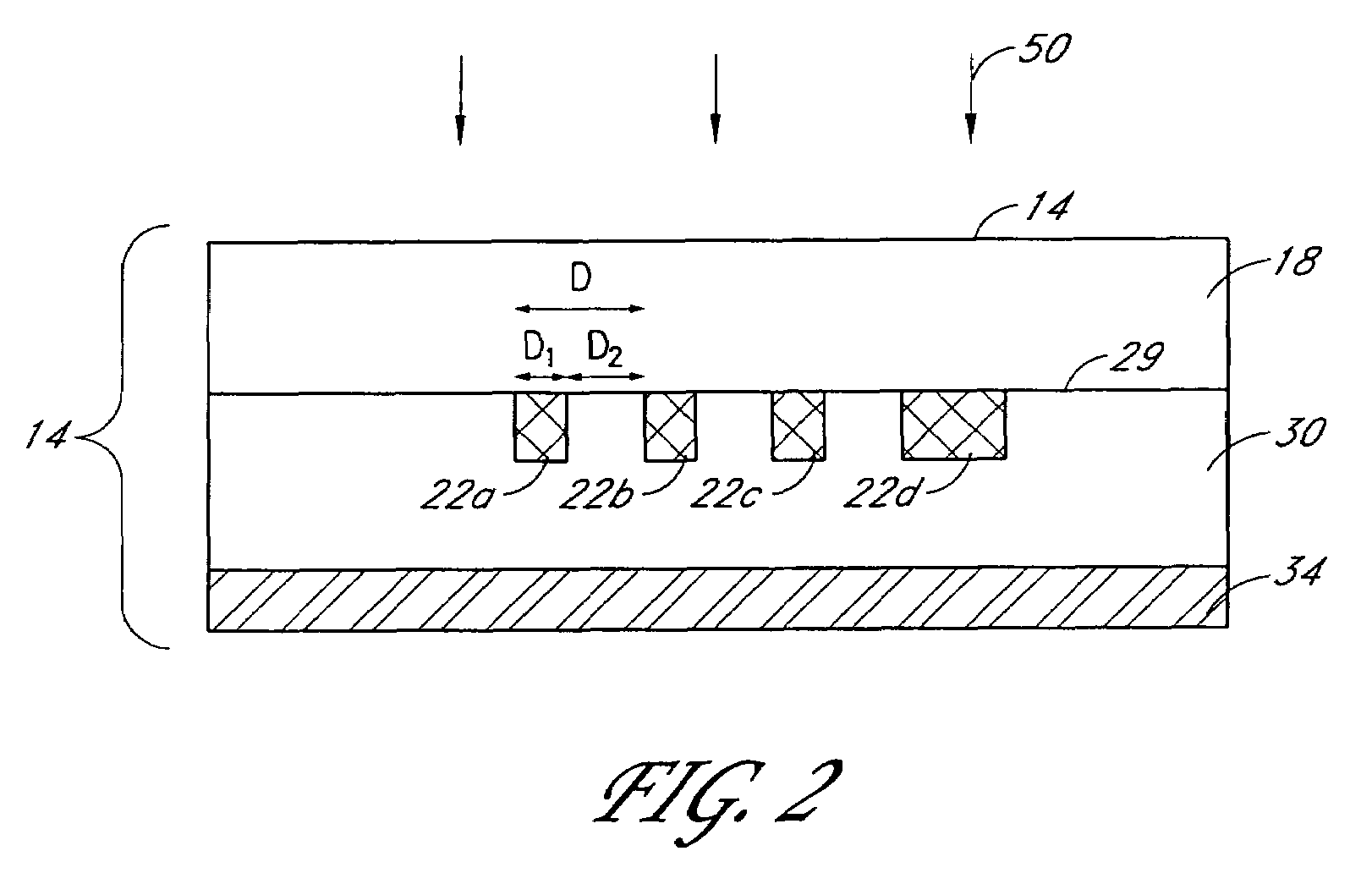
[0021]Various embodiments of the invention comprise photolithography systems that use a superlens template 14, a top view of which is shown schematically in FIG. 1. This superlens template 14 comprises a substrate 18 and a pattern 23 comprising one or more features 22 to be imaged by the photolithography system.
[0022]Images of the pattern 23 may be produced by propagating light through the superlens template 14. In certain embodiments, for example, the light may be incident on an upper surface of the template 14. The light may have an operating wavelength λ. This wavelength may correspond to a central wavelength of a wavelength band. This wavelength band may be a narrow band having a bandwidth (FWHM) of one nanometer or less or may include one or more nanometers. Suitable operating wavelengths may be in the ultraviolet and visible range of the electromagnetic spectrum from about 100 nm-800 nm, and may include, for example, the I-line of mercury lamps (λ=365 nm), krypton-fluoride exc...
PUM
 Abstract
Description
Claims
Application Information