Electron emission device with a grid electrode for focusing electron beams

a technology of electron beam and electron emission device, which is applied in the manufacture of electric discharge tubes/lamps, instruments, and discharge tubes luminescnet screens, etc., can solve the problems of complex and expensive method for assembling an electron emission device with the above described grid electrode, mis-emission of light, etc., and achieve the effect of enhancing the screen brightness

Inactive Publication Date: 2009-06-16
SAMSUNG SDI CO LTD
View PDF14 Cites 7 Cited by
  • Summary
  • Abstract
  • Description
  • Claims
  • Application Information

AI Technical Summary

Benefits of technology

[0011]In one exemplary embodiment of the present invention, an electron emission device prevents the electron emission regions from being adversely influenced by the anode electric field to inhibit the mis-emission of light due to the anode electric field, and enables elevation of the anode voltage to enhance the screen brightness.
[0012]In another exemplary embodiment of the present invention, an electron emission device has a grid electrode that can be easily aligned to a first substrate and a second substrate and can prevent the trajectory of electron beams from being deviated, thereby enhancing the screen image quality.

Problems solved by technology

However, as the voltage applied to the anode electrode is elevated, the electron emission regions are influenced by the anode electric field, and electrons are emitted from the electron emission regions even at the off-state pixels where the electron emission should not be made, thereby causing mis-emission of light.
However, with such a structure, it is very difficult to align the grid electrode between the first and second substrates in accordance with the alignment state of the first and second substrates such that the electron beam passage holes are located at their proper positions, and to assemble them with each other.
Because of this, the method for assembling an electron emission device with the above described grid electrode is complicated and expensive.
However, although the typical grid electrode may effectively shield the electron emission regions from the anode electric field, the electron beams passing through the typical grid electrode may be over-focused because the typical grid electrode is not optimized based upon its positional relation to the first and second substrates, and the voltages applied thereto, thereby deteriorating the screen image quality.

Method used


Image

  • Electron emission device with a grid electrode for focusing electron beams
  • Electron emission device with a grid electrode for focusing electron beams
  • Electron emission device with a grid electrode for focusing electron beams

Examples


Embodiment Construction

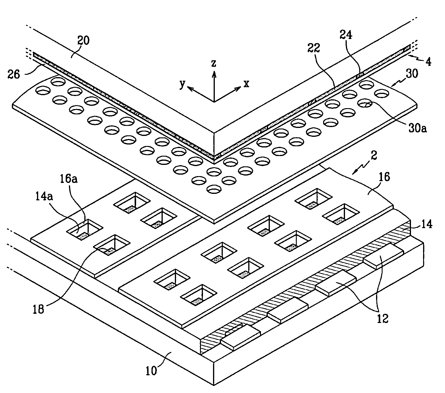
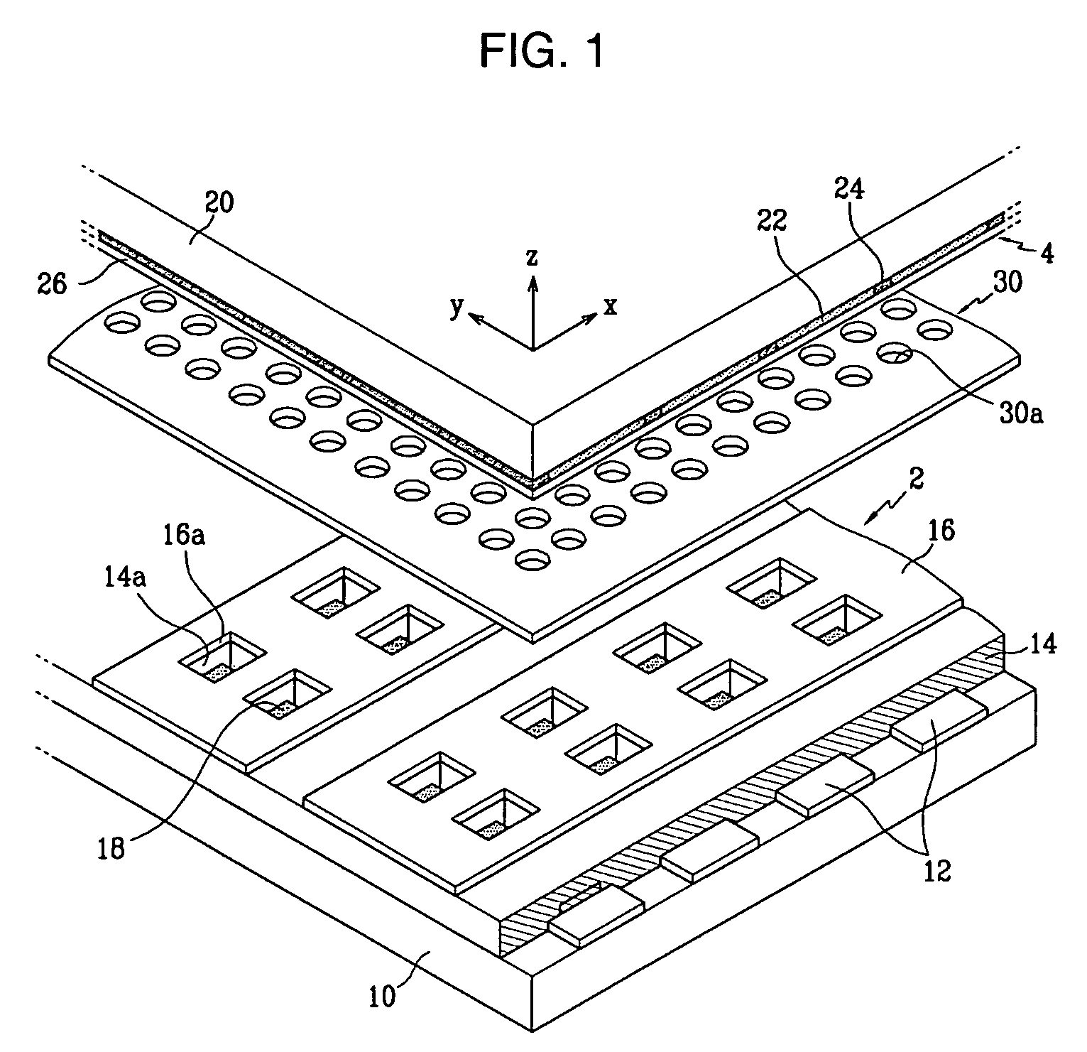
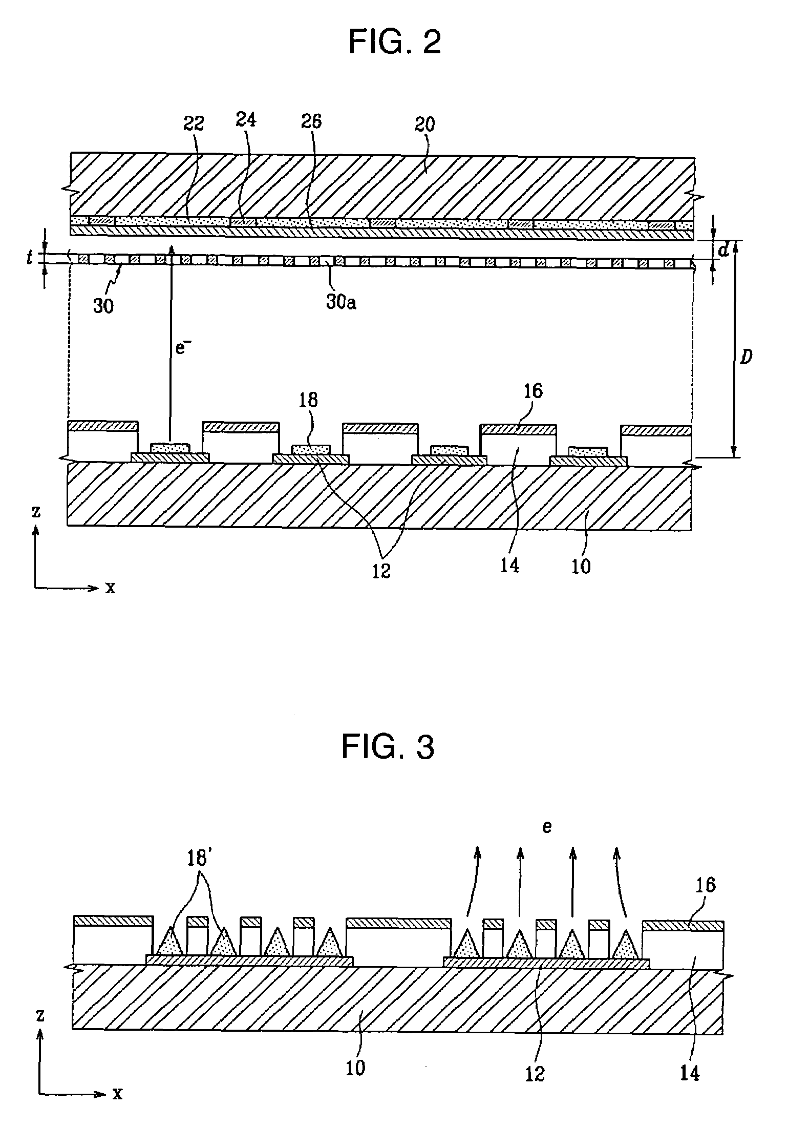
[0023]As shown in FIGS. 1 and 2, the electron emission device includes first and second substrates 10, 20 facing each with a predetermined distance therebetween to form a vacuum space. A grid electrode 30 is disposed between the substrates 10, 20. An electron emission array 2 is provided at the first substrate 10 to emit electrons toward the second substrate 20, and a light emission unit 4 is provided at the second substrate 20 to emit visible rays due to the electrons, and display the desired images.

[0024]Depending upon the type of the electron emission device, an electron emission array (e.g., the electron emission array 2) can have a different specific structure. The structure of the electron emission array 2 applied to an FEA-type electron emission device is shown in FIG. 1. However, the electron emission array of the present invention is not limited to the structure of FIG. 1, and may be altered in various manners.

[0025]Referring still to FIG. 1, a plurality of cathode electrod...


PUM


Abstract

An electron emission device includes first and second substrates facing each other while a vacuum space is interposed therebetween. An electron emission array is formed on the first substrate to emit electrons toward the second substrate, and phosphor layers are formed on the second substrate. An anode electrode is formed on a surface of the phosphor layers, and receives the voltage required for accelerating electron beams from the electron emission array. A grid electrode is disposed between the first and second substrates and is closer to the second substrate than to the first substrate. The grid electrode has electron beam passage holes, and receives a voltage lower than a location reference voltage.

Description

CROSS REFERENCE TO RELATED APPLICATION[0001]This application claims priority to and the benefit of Korean Patent Application No. 10-2004-0068573 filed on Aug. 30, 2004 in the Korean Intellectual Property Office, the entire content of which is incorporated herein by reference.BACKGROUND OF THE INVENTION[0002](a) Field of the Invention[0003]The present invention relates to an electron emission device, and in particular, to an electron emission device with a grid electrode which focuses the electron beams emitted from the electron emission regions, and prevents the electron emission regions from being adversely influenced by the anode electric field.[0004](b) Description of Related Art[0005]Generally, electron emission devices can be classified into two types. A first type uses a hot cathode as an electron emission source, and a second type uses a cold cathode as the electron emission source.[0006]Also, in the second type electron emission devices, there are a field emitter array (FEA)...

Claims


Application Information

Patent Timeline
Patent Type & Authority Patents(United States)
IPC IPC(8): H01J1/30H01J9/02
CPCH01J29/467H01J31/127H01J63/04H01J1/304
Inventor LEE, SEUNG-HYUN
Owner SAMSUNG SDI CO LTD
Why Eureka
Try Eureka