Package structure

a packaging structure and packaging technology, applied in the field of packaging structure, can solve the problems of large overall volume of the conventional structure, inability to manufacture the conventional package structure b>100/b>, and relatively high manufacturing cost of the conventional package structure, so as to achieve the effect of small thermal resistance, high wiring density, and reduced manufacturing cos

Active Publication Date: 2009-06-23
CYNTEC
View PDF18 Cites 5 Cited by
  • Summary
  • Abstract
  • Description
  • Claims
  • Application Information

AI Technical Summary

Benefits of technology

[0024]Based on the above description, since the second electronic components with greater heat generation rate are disposed on the second carrier with smaller thermal resistance, heat generated by the second electronic components during the operation of the package structure is directly transferred to a next level electronic device via the second carrier, such that the package structure will not be too hot to work normally. Furthermore, due to the relatively high wiring density in the first carrier, more first electronic components can be disposed on the first carrier, thereby making full use of the disposing space of the first carrier.

Problems solved by technology

However, the electronic components 120 of the conventional package structure 100 are all small sized first-level packages and the area for wiring on the surface 112 of the PCB 110 is limited, thereby resulting in a relatively large overall volume of the conventional structure 100.
Additionally, since the electronic components 120 are required to be formed through a first-level packaging process, the manufacturing cost of the conventional package structure 100 is relatively high.
Moreover, the package structure 100 must be manually inserted into the next level electronic device, so that both of them cannot be assembled together through an automatic machine.
Therefore, the conventional package structure 200 has poor heat dissipation capacity.

Method used


Image

  • Package structure
  • Package structure
  • Package structure

Examples


first embodiment

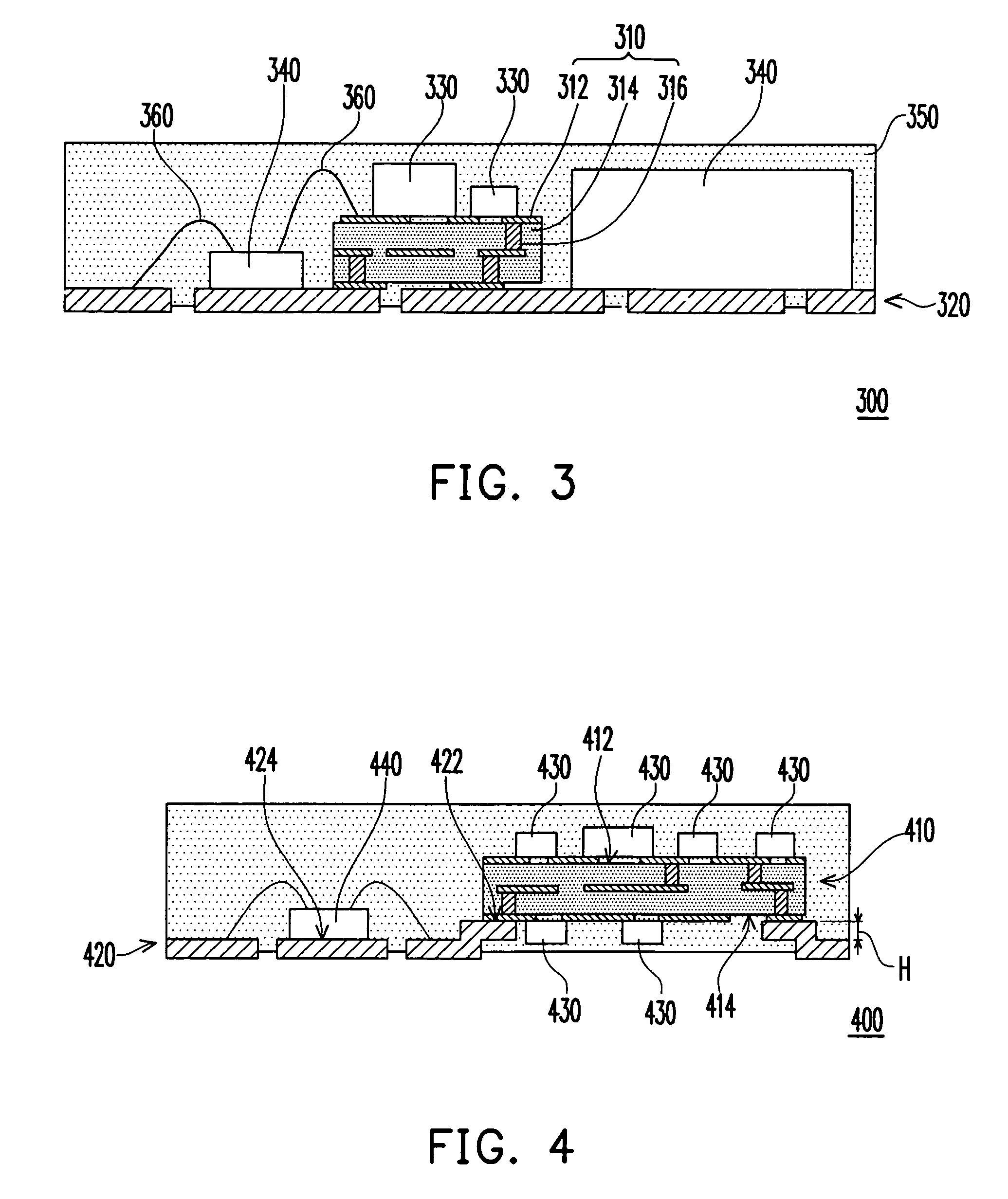
[0034]Referring FIG. 3, it is a schematic sectional view of a package structure according to the first embodiment of the present invention. The package structure 300 in the first embodiment comprises a first carrier 310, a second carrier 320, at least a first electronic component 330 (for example, two first electronic components are shown in FIG. 3), and at least a second electronic component 340 (for example, two second electronic components are shown in FIG. 3). The second carrier 320 is electrically connected to the first carrier 310, and the thermal resistance of the first carrier 310 may be greater than that of the second carrier 320. The first electronic components 330 are disposed on the first carrier 310 and electrically connected to the first carrier 310. The second electronic components 340 are disposed on the second carrier 320 and electrically connected to the second carrier 320. The heat generation rate of each first electronic component 330 may be smaller than that of ...

second embodiment

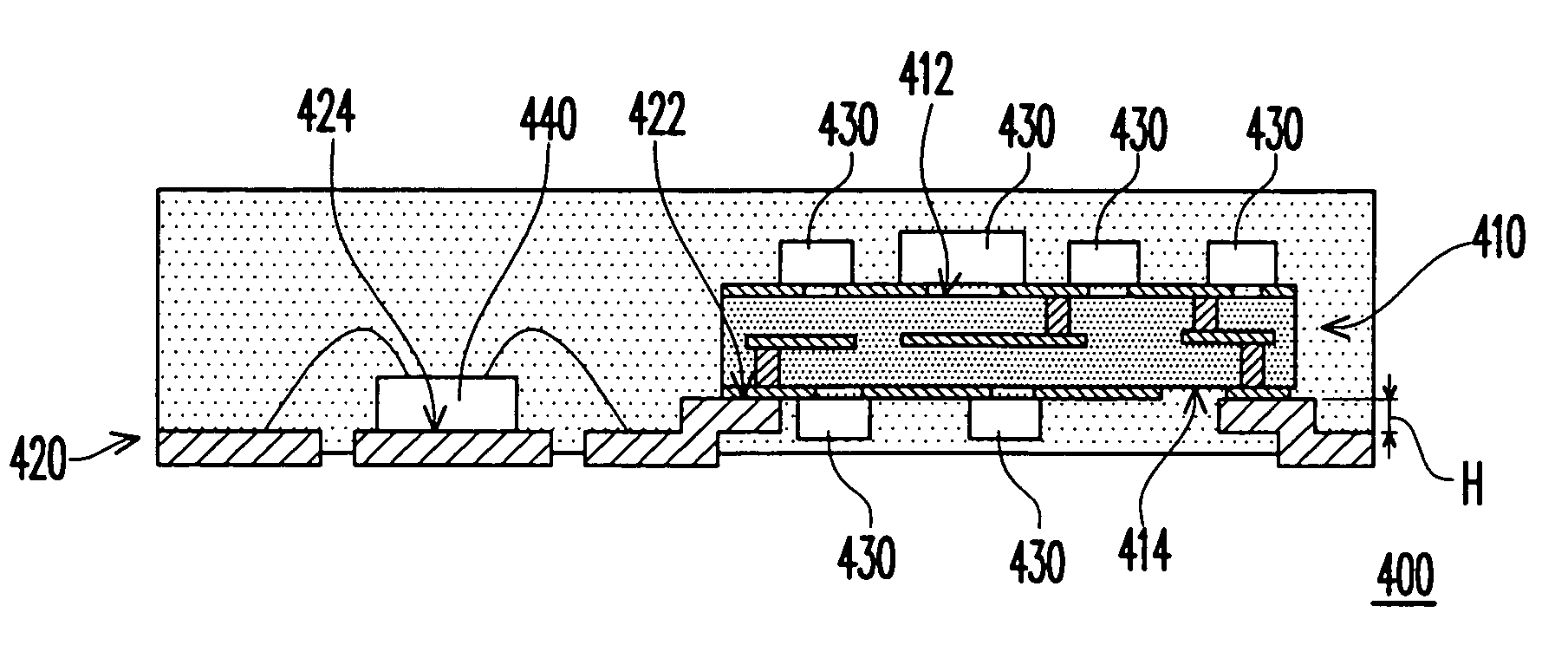
[0039]Referring to FIGS. 3 and 4, FIG. 4 is a schematic sectional view of a package structure according to the second embodiment of the present invention. The package structure 400 in the second embodiment mainly differs from the package structure 300 in the first embodiment in that, the first electronic components 430 may be disposed on two opposite surfaces 412 and 414 of the first carrier 410. In the second embodiment, the first carrier 410 may be still disposed on the second carrier 420. The second carrier 420 comprises a first carrying area 422 and a second carrying area 424, which are not in the same plane. Particularly, as for the relative position shown in FIG. 4, there is a height difference H between the second carrying area 424 and the first carrying area 422. Additionally, the first carrier 410 is disposed on the first carrying area 422 and the second electronic components 440 are disposed on the second carrying area 424.

[0040]Since the first electronic components 430 ar...

third embodiment

[0041]Referring to FIGS. 3, 4, and 5, FIG. 5 is a schematic sectional view of a package structure according to the third embodiment of the present invention. The package structure 500 in the third embodiment mainly differs from the package structures 300 and 400 in the above-mentioned embodiments in that, the first carrier 510 in the third embodiment may be disposed beside the second carrier 520. Additionally, the package structure 500 further comprises at least one bonding wire 560 (three bonding wires are shown in FIG. 5) and the first carrier 510 is electrically connected to the second carrier 520 via at least one of the bonding wires 560. Additionally, the first carrier 510 comprises a plurality of bonding pads 516 disposed on a surface 514 of the first carrier 510 and exposed outside the encapsulant 550. Compared with the above-mentioned embodiments, the bonding pads 516 exposed outside the encapsulant 550 in the third embodiment are used for transmitting electric signals to th...


PUM

PropertyMeasurementUnit
thermal resistanceaaaaaaaaaa
heat generation rateaaaaaaaaaa
carrying areaaaaaaaaaaa

Abstract

A package structure including a first carrier, a second carrier, at least a first electronic component and at least a second electronic component is provided. The second carrier is electrically connected to the first carrier. The first electronic component is disposed on the first carrier and electrically connected to the first carrier. The second electronic component is disposed on the second carrier and electrically connected to the second carrier.

Description

CROSS-REFERENCE TO RELATED APPLICATION[0001]This application claims the priority benefit of Taiwan application serial no. 95115846, filed on May 4, 2006. All disclosure of the Taiwan application is incorporated herein by reference.BACKGROUND OF THE INVENTION[0002]1. Field of Invention[0003]The present invention relates to a package structure, and more particularly, to a package structure with a plurality of carriers.[0004]2. Description of Related Art[0005]A package structure is a product formed through complicated packaging processes. Various package structures have different electrical performances and heat dissipation capacities, and a designer may select a package structure with suitable electrical performance and heat dissipation capacity according to design requirements.[0006]Referring to FIG. 1, it is a schematic view of a conventional package structure. The conventional package structure 100 comprises a printed circuit board (PCB) 110 and a plurality of electronic components...

Claims


Application Information

Patent Timeline
Patent Type & Authority Patents(United States)
IPC IPC(8): H05K7/00
CPCH01L23/3107H01L23/49531H01L23/49575H01L24/49H01L2924/1305Y10T29/49121H01L2924/1306H01L2924/014H01L24/48H01L2924/19107H01L2924/13091H01L2924/13055H01L2224/4911H01L2224/48247H01L2224/48091H01L2924/00014H01L2924/00H01L2924/181H01L2224/45099H01L2224/05599H01L2924/00012
Inventor CHEN, DA-JUNGLIN, YI-CHENGLU, BAU-RUFANG, YI-MINWEN, CHAU-CHUNLIU, CHUN-TIAO
Owner CYNTEC
Why Eureka
Try Eureka