Supercharge Your Innovation With Domain-Expert AI Agents!

Semiconductor device and method of manufacturing the same

a semiconductor device and semiconductor technology, applied in the field of semiconductor devices, can solve the problems of etching of the surficial portion of the semiconductor device, adversely affecting the degree of integration and micronization, so as to improve the degree of integration, the restriction of the design basis can be relaxed, and the resistivity is large.

Inactive Publication Date: 2009-07-07
RENESAS ELECTRONICS CORP
View PDF2 Cites 0 Cited by
  • Summary
  • Abstract
  • Description
  • Claims
  • Application Information

AI Technical Summary

Benefits of technology

The present invention provides a semiconductor device and a method of manufacturing the same that protects the surface of the semiconductor substrate during the formation of contact holes and reduces the risk of etching the surface of the semiconductor substrate. This is achieved by using a protective film that is formed below the connecting portion of the contact and the gate electrode. This protective film helps to relax restrictions on the design basis, allowing improvement in the degree of integration and micronization of the semiconductor device.

Problems solved by technology

However, the conventional solution by widening the gate electrodes in the connecting portions of the gate electrodes and the contacts has inevitably resulted in restrictions on the design basis, adversely affecting improvement in the degree of integration and micronization.
H11-195704, if the contact is formed wider than the gate electrode, there is a danger that the surficial portion of the semiconductor device is etched when forming the contact hole.

Method used


Image

  • Semiconductor device and method of manufacturing the same
  • Semiconductor device and method of manufacturing the same
  • Semiconductor device and method of manufacturing the same

Examples


Embodiment Construction

[0042]The invention will be now described herein with reference to an illustrative embodiment. Those skilled in the art will recognize that many alternative embodiments can be accomplished using the teachings of the present invention and that the invention is not limited to the embodiment illustrated for explanatory purposes.

[0043]Paragraphs below will explain embodiments of the present invention, referring to the attached drawings. It is to be understood that any similar constituents will be given with similar reference numerals, and detailed explanations therefor will not be repeated.

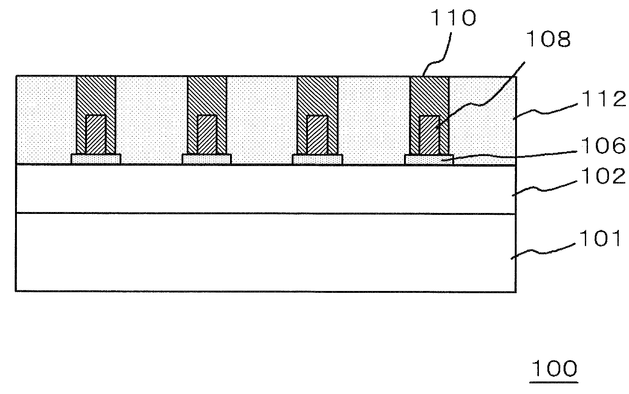
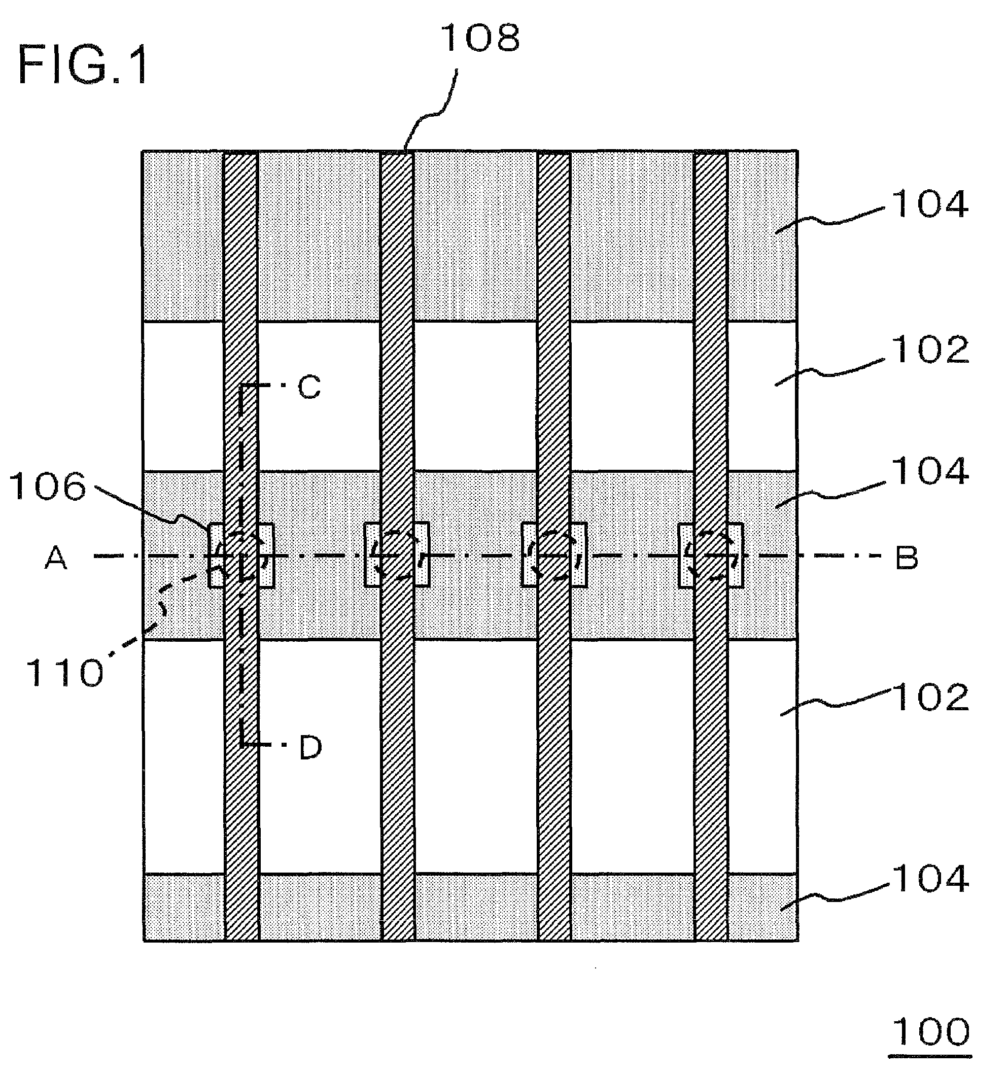
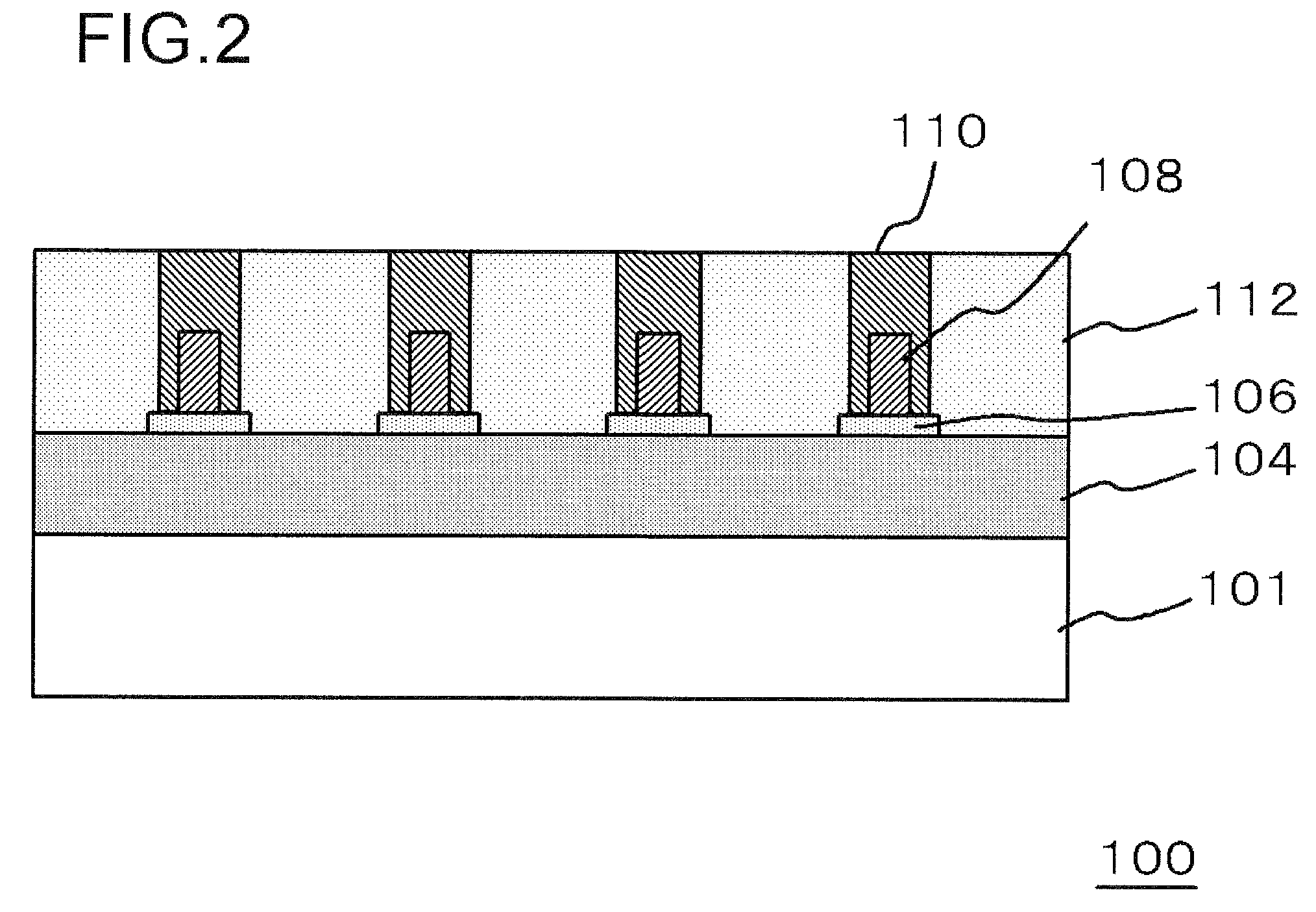
[0044]FIG. 1 is a plan view showing a configuration of a semiconductor device 100 according to this embodiment. FIG. 2 is an A-B sectional view of FIG. 1.

[0045]The semiconductor device 100 has a semiconductor substrate 101, impurity-diffused regions 102 and device isolation insulating films 104 (isolation regions) formed in the surficial portion of the semiconductor substrate 101. In the description b...


PUM


Abstract

A semiconductor device has a semiconductor substrate having an impurity-diffused region and a device isolation insulating film formed in the surficial portion thereof, a gate electrode formed on the semiconductor substrate, a contact formed on the gate electrode and connected to the gate electrode, and a protective film disposed between the semiconductor substrate and the gate electrode, below the connecting portion between the gate electrode and the contact, formed wider in width than the gate electrode in a sectional view taken along the direction of gate length of the gate electrode.

Description

[0001]This application is based on Japanese patent application No. 2006-212445 the content of which is incorporated hereinto by reference.BACKGROUND[0002]1. Technical Field[0003]The present invention relates to a semiconductor device and a method of manufacturing the same, and more specifically to a semiconductor device containing a gate electrode and a contact connected to the gate electrode.[0004]2. Related Art[0005]Japanese Laid-Open Patent Publication No. H5-48022 describes a configuration in which a common gate electrode is disposed as extending over a P-type diffusion region composing a P-channel MOS transistor and an N-type diffusion region composing an N-channel MOS transistor, wherein the gate electrode is widened in the portion thereof which falls between the P-type diffusion region and the N-type diffusion region, as compared with the portion thereof which falls on these diffusion regions, and a contact connecting the gate electrode and an interconnect formed on the upper...

Claims


Application Information

Patent Timeline
Patent Type & Authority Patents(United States)
IPC IPC(8): H01L23/62
CPCH01L21/76816
Inventor FUKUI, TAKAMICHI
Owner RENESAS ELECTRONICS CORP
Features
  • R&D
  • Intellectual Property
  • Life Sciences
  • Materials
  • Tech Scout
  • Unparalleled Data Quality
  • Higher Quality Content
  • 60% Fewer Hallucinations
Learn More