Semiconductor substrate, electronic device and method for manufacturing semiconductor substrate
a semiconductor substrate and electronic device technology, applied in the direction of semiconductor devices, semiconductor/solid-state device details, electrical apparatus, etc., can solve the problems of instable operation of semiconductor devices and further decrease of resistivity, and achieve high resistance, high resistance, and high resistance layer
- Summary
- Abstract
- Description
- Claims
- Application Information
AI Technical Summary
Benefits of technology
Problems solved by technology
Method used
Image

Examples
embodiment examples
Embodiment Example 1
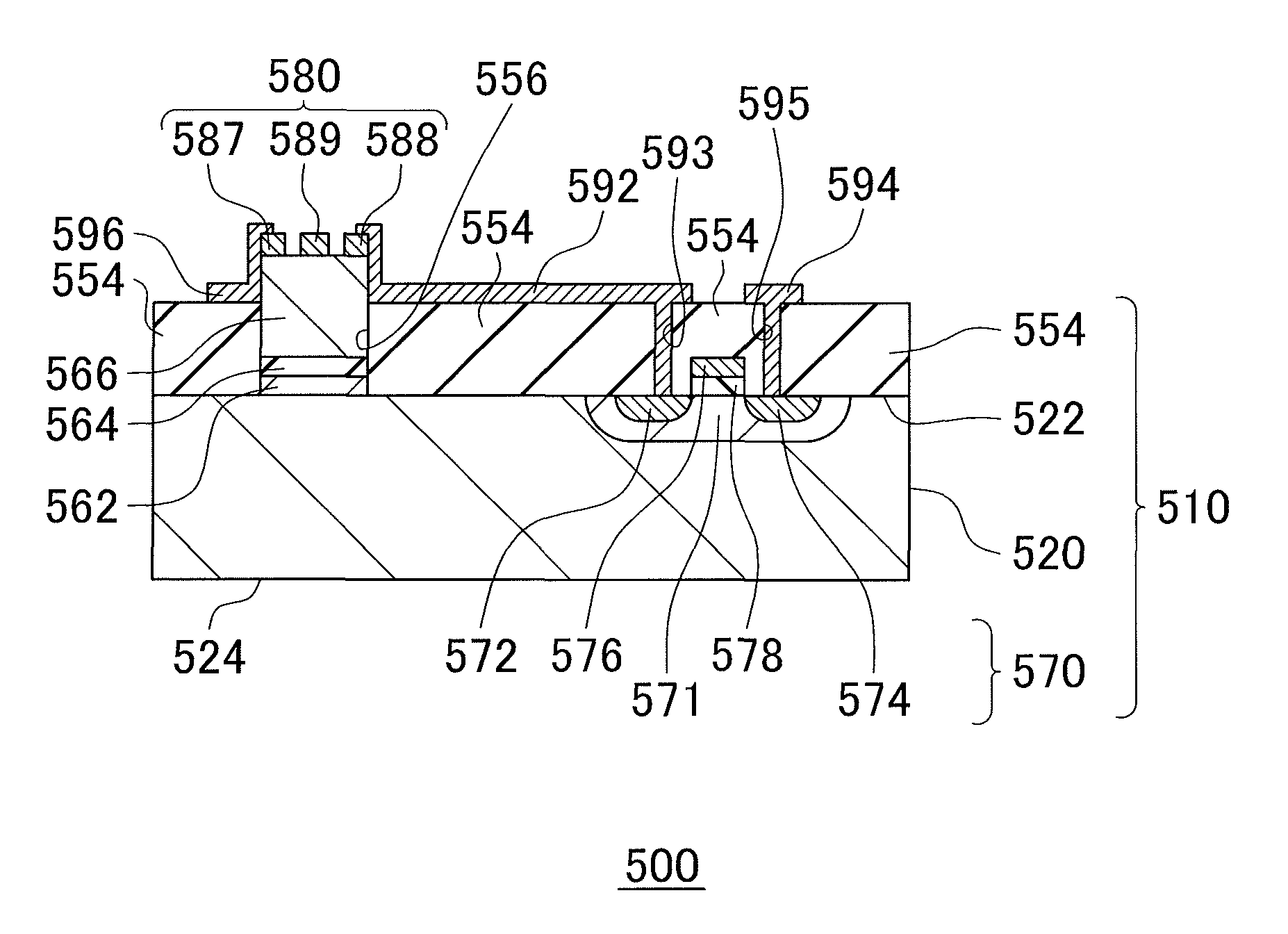
[0106]An electronic device 500 was fabricated according to the procedure shown in FIG. 6. A commercially-available SOI wafer was prepared as the base wafer 520. As a first electronic element 570, a MOSFET was formed on the Si crystal layer of the base wafer 520. The wafer 710 was prepared in this way. As an inhibition layer 554, a SiO2 layer was formed by CVD to be in contact with the first main plane 522 of the base wafer 520. The average thickness of the SiO2 layer was 1 μm. An opening 556 was formed through a part of the inhibition layer 554 by lithography. The size of the opening 556 was set to be 15 μm×15 μm.
[0107]Thus formed wafer 710 was placed inside the reaction chamber, and a Ge crystal layer was formed as a seed crystal 562. The Ge crystal layer was selectively formed inside the opening 556 by CVD. The Ge crystal layer is formed by first depositing about 20 nm under a condition of the source gas being GeH4, the pressure in the reaction chamber being 2....
embodiment example 2
[0114]A semiconductor wafer 510 was fabricated just as in Embodiment Example 1, except that an AlGaAs layer that has an Al composition of 0.3 with respect to the total of Al and Ga and that includes oxygen in an atomic concentration of about 5×10¹⁹ / cm3 was used as the high resistance layer 564, instead of using the selectively oxidized AlGaAs layer. Dibutyl ether was used as the oxygen source. The dibutyl ether was obtained by adding, to the source gas, hydrogen aerated through the dibutyl ether liquid maintained to 25 degrees centigrade in a flow rate of 200 cc / minute, and supplied during the crystal growth of the AlGaAs layer. The above-described oxygen concentration was achieved in this method. The other procedures are the same as adopted in Embodiment Example 1.
[0115]The leak current between the collector electrodes in the plurality of HBTs respectively formed in the openings adjacent to each other was observed to be extremely low (1.3×10⁻⁸ A on average for 10V applied voltage)....
embodiment example 3
[0116]A semiconductor wafer 510 was fabricated just as in Embodiment Example 1, except that an InGaP layer that includes boron in an atomic concentration of about 2×10²⁰ / cm3 was used as the high resistance layer 564, instead of using the selectively oxidized AlGaAs layer. Trimethyl boron was used as the boron source. The trimethyl boron was obtained by adding, to the source gas, hydrogen aerated through the trimethyl boron liquid maintained to 10 degrees centigrade in a flow rate of 10 cc / minute, and supplied during the crystal growth of the InGaP layer. The above-described boron concentration was achieved in this method. The other procedures are the same as adopted in Embodiment Example 1.
[0117]The leak current between the collector electrodes in the plurality of HBTs respectively formed in the openings adjacent to each other was observed to be extremely low (2.7×10⁻⁹ A on average for 10V applied voltage). As clear from the above, obtained are a semiconductor wafer and an electroni...
PUM
 Abstract
Description
Claims
Application Information