Method for forming semiconductor device having fin structure

a technology of semiconductor devices and fins, applied in the direction of semiconductor devices, basic electric elements, electrical equipment, etc., can solve the problems of complex process and degraded accuracy, and achieve the effect of simplifying the process and maximizing the current driving operation

Inactive Publication Date: 2009-07-28
SK HYNIX INC
View PDF17 Cites 4 Cited by
  • Summary
  • Abstract
  • Description
  • Claims
  • Application Information

AI Technical Summary

Benefits of technology

[0011]Various embodiments of the present invention are directed at providing a method for forming a semiconductor device having a fin structure that comprises etching a silicon substrate using a recess gate mask and performing a selective etching process on a device isolation film having a double oxide film structure with a rapid oxide film etching speed and a slow oxide film etching speed, thereby simplifying the process and maximizing a current driving operation.

Problems solved by technology

Furthermore, since the recess gate mask and the fin mask are both used, the process is complicated, and accuracy is degraded.

Method used


Image

  • Method for forming semiconductor device having fin structure
  • Method for forming semiconductor device having fin structure
  • Method for forming semiconductor device having fin structure

Examples


Embodiment Construction

[0017]The present invention will be described in detail with reference to the accompanying drawings. Wherever possible, the same reference numbers will be used throughout the drawings to refer to the same or like parts.

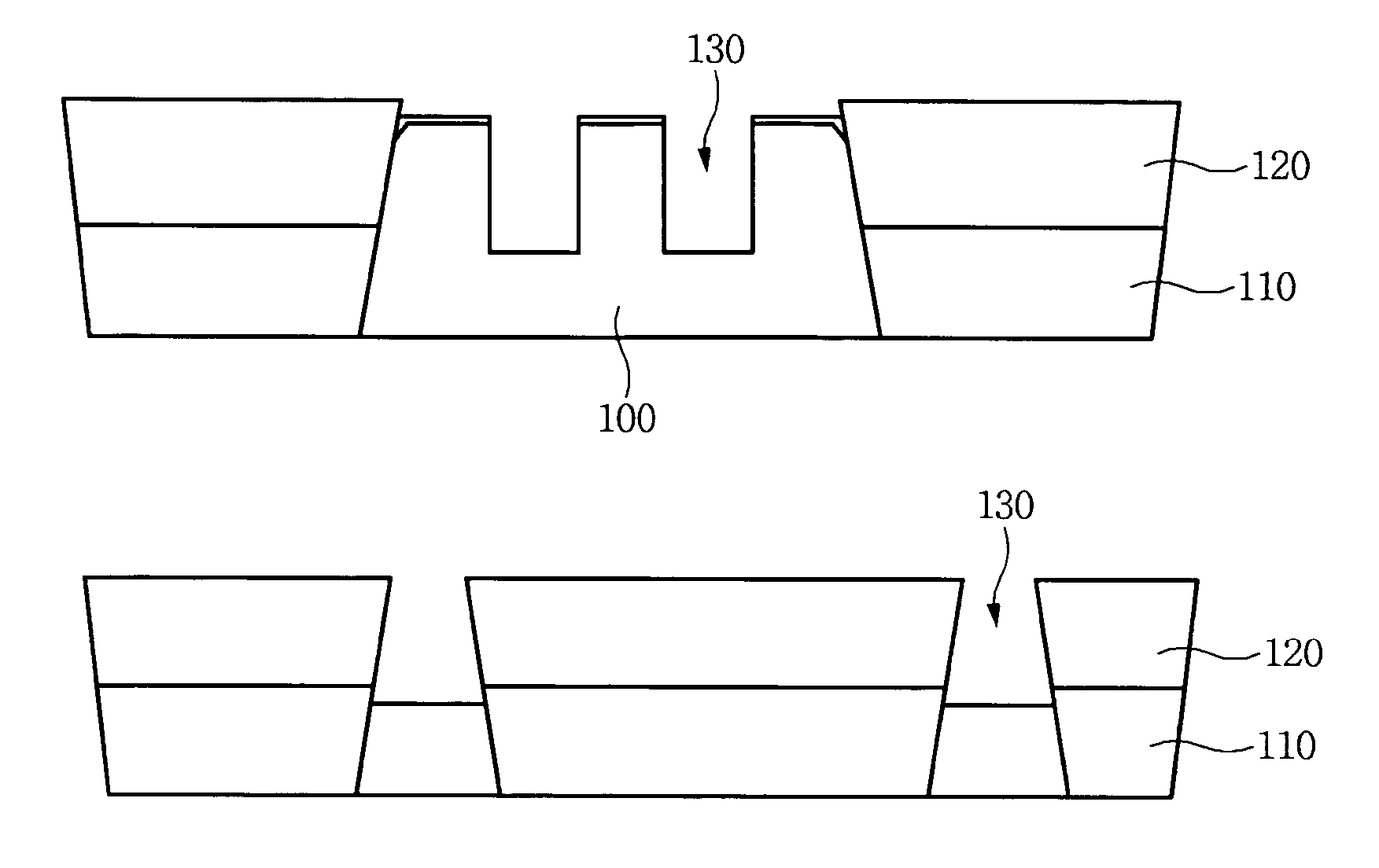
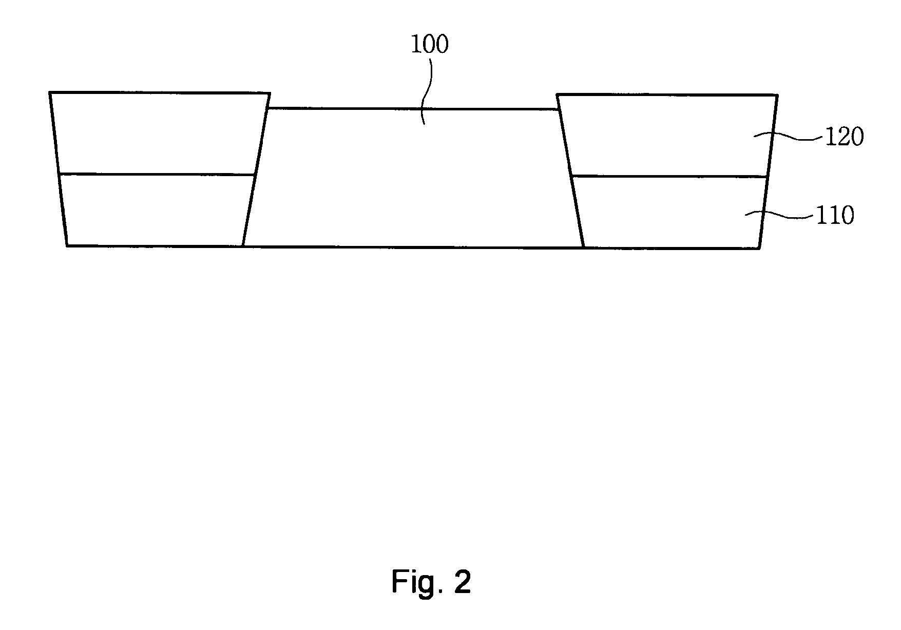
[0018]Referring to FIG. 2, a region for forming a device isolation film over a silicon substrate is etched to define an active area 100, and a first oxide film 110 and a second oxide film 120 are sequentially deposited thereon to form a double oxide film.

[0019]Preferably, the thickness of the first oxide film (110) and the second oxide film (120) ranges from 300 to 3000 Å.

[0020]Preferably, the first oxide film 110 includes an oxide film having a rapid wet-etching speed, and the second oxide film 120 includes an oxide film having a slow wet-etching speed. Preferably, the oxide film having a rapid wet-etching speed includes a SOD (spin on dielectric) oxide film, and the oxide film having a slow wet-etching speed includes a HDP (high density plasma) oxide film.

[0021]Refe...


PUM


Abstract

A method for forming a semiconductor device having a fin structure includes (a) forming a device isolation film over a silicon substrate to define an active area, (b) etching silicon substrate of gate forming region to form a trench, (c) selectively etching the device isolation film of a trench boundary, (d) forming a gate oxide film over the entire surface of the resulting structure, (e) depositing an electrode material over the entire surface of the resulting structure to form a gate electrode, and (f) forming a gate spacer over a sidewall of the gate electrode.

Description

BACKGROUND OF THE INVENTION[0001]1. Field of the Invention[0002]The present invention generally relates to a method for forming a semiconductor device having a fin structure, and more specifically, to a method for forming a semiconductor device having a fin structure which comprises etching a silicon substrate with a recess gate mask and performing a selective etching process on a device isolation film having a double oxide film structure.[0003]2. Description of the Related Art[0004]A conventional method for forming a semiconductor device having a fin structure is performed as follows.[0005]First, a device isolation oxide film is formed over a silicon substrate, and then ions are implanted into a cell region to form a well.[0006]The silicon substrate of an active area is etched using a recess gate mask.[0007]The device isolation oxide film is etched using a fin mask.[0008]A gate oxide film is formed over the entire surface of the resulting structure.[0009]A polysilicon layer, a tung...

Claims


Application Information

Patent Timeline
Patent Type & Authority Patents(United States)
IPC IPC(8): H01L21/336
CPCH01L29/7851H01L29/66795H01L29/66621H01L21/18
Inventor KIM, YOUNG BOG
Owner SK HYNIX INC
Why Eureka
Try Eureka