

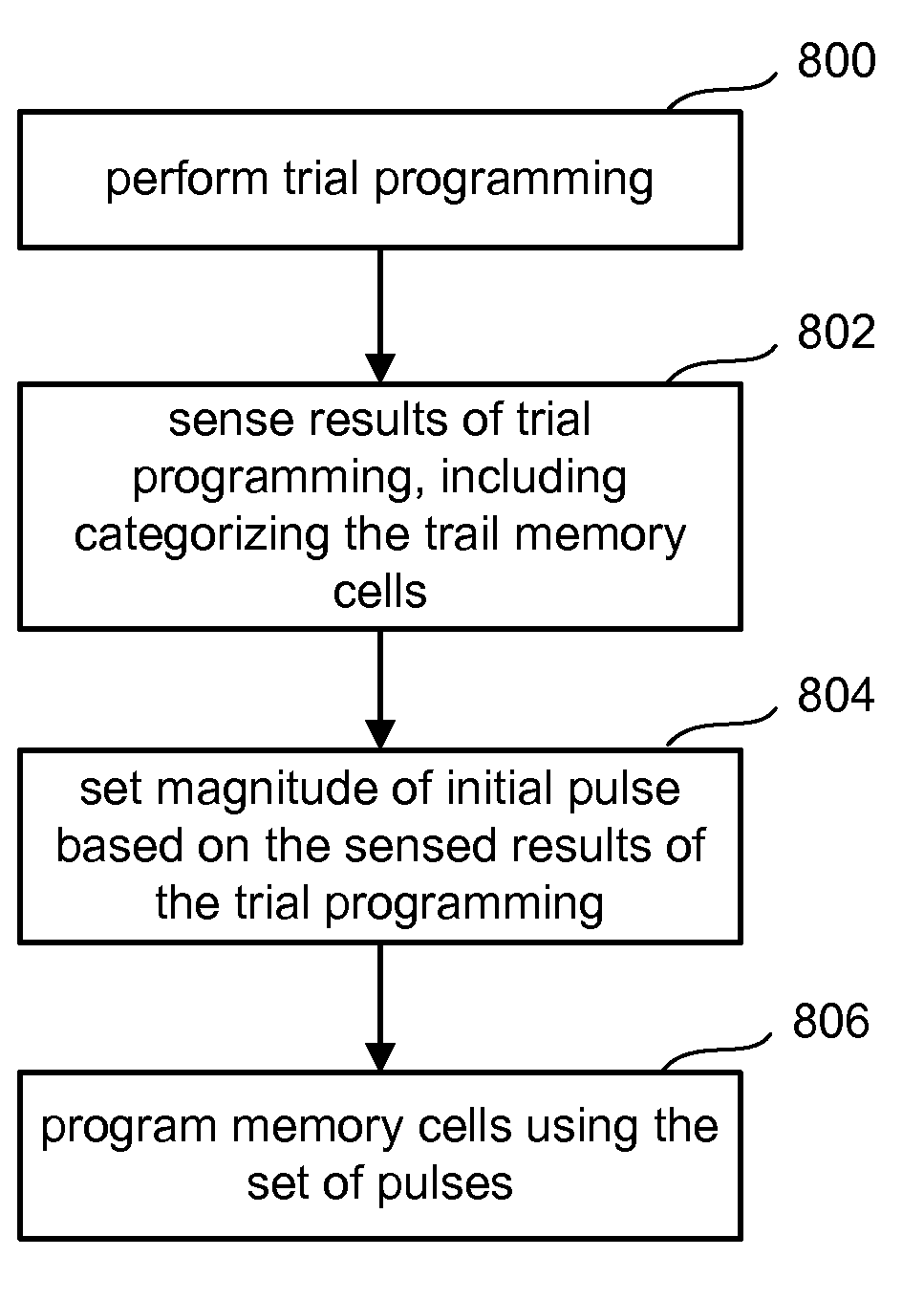
Non-volatile storage system with initial programming voltage based on trial
a non-volatile storage and voltage technology, applied in static storage, digital storage, instruments, etc., can solve the problems of memory cells being over-programmed, longer programming time, and charge becoming trapped in the insulation between the floating gate and the channel region
- Summary
- Abstract
- Description
- Claims
- Application Information
AI Technical Summary
Benefits of technology
Problems solved by technology
Method used
Image

Examples
Embodiment Construction
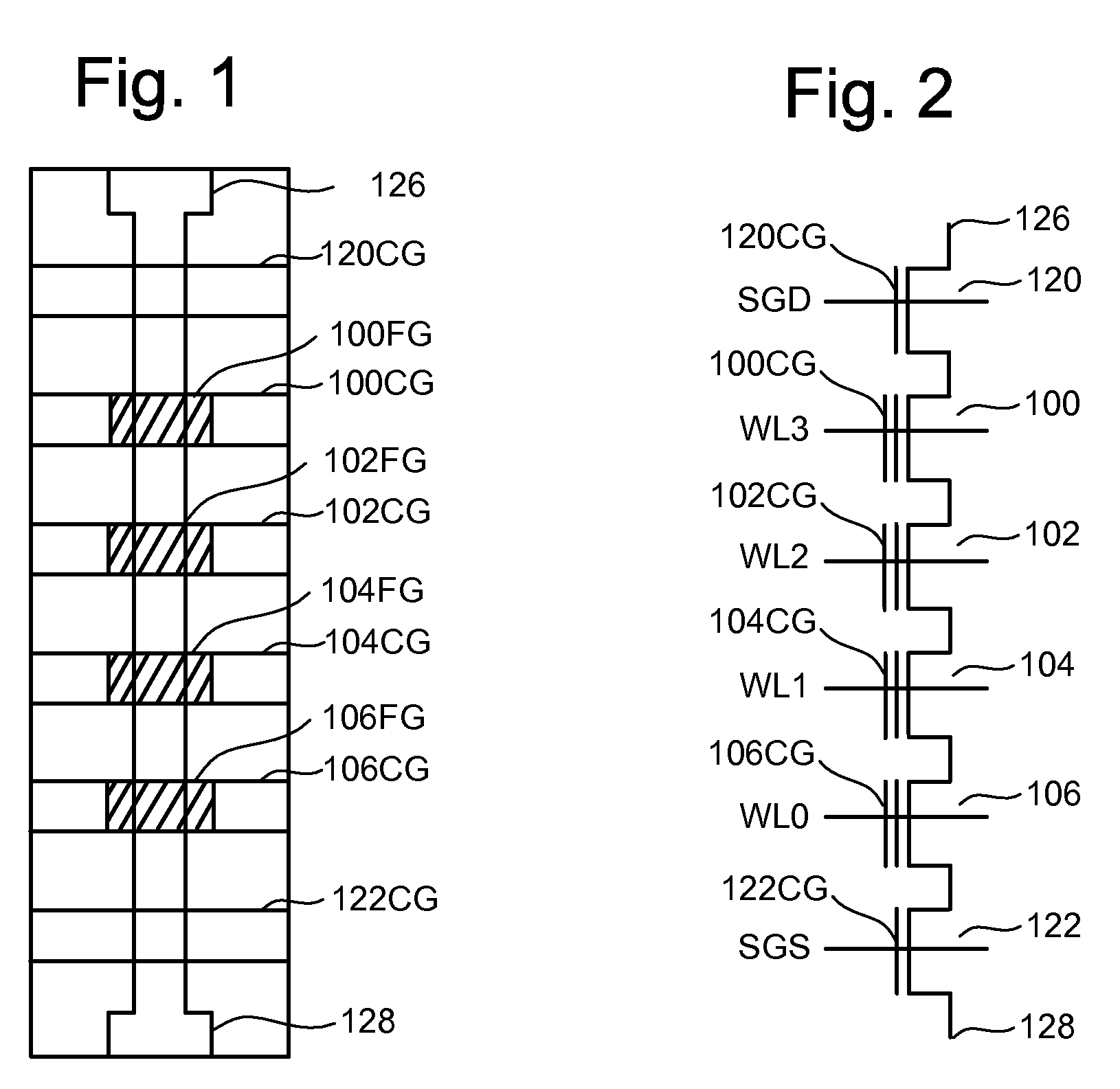
[0035]One example of a flash memory system uses the NAND structure, which includes arranging multiple transistors in series, sandwiched between two select gates. The transistors in series and the select gates are referred to as a NAND string. FIG. 1 is a top view showing one NAND string. FIG. 2 is an equivalent circuit thereof. The NAND string depicted in FIGS. 1 and 2 includes four transistors 100, 102, 104 and 106 in series and sandwiched between a first (or drain side) select gate 120 and a second (or source side) select gate 122. Select gate 120 connects the NAND string to a bit line via bit line contact 126. Select gate 122 connects the NAND string to source line 128. Select gate 120 is controlled by applying the appropriate voltages to select line SGD. Select gate 122 is controlled by applying the appropriate voltages to select line SGS. Each of the transistors 100, 102, 104 and 106 has a control gate and a floating gate. For example, transistor 100 has control gate 100CG and ...
PUM
 Abstract
Description
Claims
Application Information