Derivative superposition circuit for linearization

a superposition circuit and linearization technology, applied in the field of derivative superposition circuits for linearization, can solve problems such as the increase of phenomenon, and achieve the effects of stable linearization, reduced overall area of the circuit, and easy construction

Inactive Publication Date: 2009-08-04
SAMSUNG ELECTRO MECHANICS CO LTD
View PDF7 Cites 2 Cited by
  • Summary
  • Abstract
  • Description
  • Claims
  • Application Information

AI Technical Summary

Benefits of technology

[0018]An advantage of the present invention is that it provides a derivative superposition circuit for linearization, in which transistors having a different gate length, which are supported in a general CMOS process, are used so that stable linearization is possible without delicate tuning, and a plurality of transistors can be operated only by one bias voltage so that a bias circuit can be easily constructed and the overall area of the circuit can be reduced.
[0019]Additional aspects and advantages of the present general inventive concept will be set forth in part in the description which follows and, in part, will be obvious from the description, or may be learned by practice of the general inventive concept.
[0020]According to an aspect of the invention, a derivative superposition circuit for linearization includes a first active element that is provided with first to third terminals and in which the magnitude and direction of current flowing the second terminal to the third terminal changes on the basis of the magnitude of a voltage applied between the first and second terminals; and a second active element that is provided with first to third terminals and has complementary characteristics with the first active element. The first terminals of the first and second active elements are connected to each other so that a predetermined operational bias voltage is maintained by first and second power supplies through a first impedance, and are connected to an input end through a second impedance. The third terminals of the first and second active elements are connected to an output end, and the second terminals of the first and second active elements are connected to the second power supply through a third impedance.
[0021]The first power supply is a voltage power supply which supplies a predetermined positive voltage applied between the first and second terminals, and the second power supply is a ground power supply.
[0022]The first, second and third terminals of the first and second active elements are a gate, source, and drain, respectively.
[0023]The gate lengths of the first and second active elements are different from each other, and the gate length of the first active element is shorter than the gate length of the second active element.

Problems solved by technology

Accordingly, such a phenomenon increases where undesired signals are interfered with each other.
However, since transmitters and receivers which are used in most of real communication systems are implemented of non-linearized circuits, such problems occur, which are caused by the mixture and modulation between signals generated while the signals pass through the non-linearized systems.

Method used


Image

  • Derivative superposition circuit for linearization
  • Derivative superposition circuit for linearization
  • Derivative superposition circuit for linearization

Examples


Embodiment Construction

[0036]Reference will now be made in detail to the embodiments of the present general inventive concept, examples of which are illustrated in the accompanying drawings, wherein like reference numerals refer to the like elements throughout. The embodiments are described below in order to explain the present general inventive concept by referring to the figures.

[0037]Hereinafter, a preferred embodiment of the present invention will be described in detail with reference to the accompanying drawings.

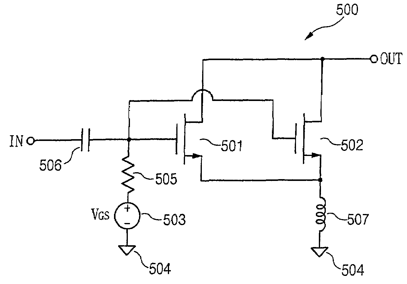
[0038]FIG. 5 is a circuit diagram showing a derivative superposition circuit 500 according to the present invention. As shown in FIG. 5, the derivative superposition circuit 500 includes a first active element 501 and a second active element 502 having a complementary characteristic with respect to the first active element 501.

[0039]The first active element 501 is provided with a gate, source, and drain. In accordance with the magnitude and polarity of a voltage applied to the gate and source...


PUM


Abstract

A derivative superposition circuit for linearization includes a first active element that is provided with first to third terminals and in which the magnitude and direction of current flowing from the second terminal to the third terminal changes on the basis of the magnitude of a voltage applied between the first and second terminals; and a second active element that is provided with first to third terminals and has complementary characteristics with the first active element. The first terminals of the first and second active elements are connected to each other so that a predetermined operational bias voltage is maintained by first and second power supplies through a first impedance, and are connected to an input end through a second impedance. The third terminals of the first and second active elements are connected to an output end, and the second terminals of the first and second active elements are connected to the second power supply through a third impedance.

Description

CROSS-REFERENCE TO RELATED APPLICATIONS[0001]The application claims the benefit of Korea Patent Application No. 2005-0075165 filed with the Korea Industrial Property Office on Aug. 17, 2005, the disclosure of which is incorporated herein by reference.BACKGROUND OF THE INVENTION[0002]1. Field of the Invention[0003]The present invention relates to a derivative superposition circuit for linearization, in which transistors having a different gate length, which are supported in a general CMOS process, are used so that stable linearization is possible without delicate tuning, and a plurality of transistors can be operated only by one bias voltage so that a bias circuit can be easily constructed and the overall area of the circuit can be reduced.[0004]2. Description of the Related Art[0005]Recently, wireless communication systems with various purposes are commonly used through standardization. Accordingly, such a phenomenon increases where undesired signals are interfered with each other.[...

Claims


Application Information

Patent Timeline
Patent Type & Authority Patents(United States)
IPC IPC(8): H04B1/10H04B1/04
CPCH03F1/3252H03K17/00H03K17/30
Inventor NA, YOO SAMKIM, BYUNG SUNGBAEK, WON JINKIM, MOON SUN
Owner SAMSUNG ELECTRO MECHANICS CO LTD
Why Eureka
Try Eureka