Multilayer ultrasonic transducer and method for manufacturing same

a transducer and multi-layer technology, applied in the direction of mechanical vibration separation, device material selection, curling-tongs, etc., can solve the problems of deterioration of the sensitivity of the transducer, the mismatch between the electrical impedance the rise of the ultrasonic transducer and the ultrasonic image diagnostic system, so as to improve the vibration feature, wide bandwidth, and high sensitivity

Active Publication Date: 2009-08-11
HUMANSCAN
View PDF5 Cites 9 Cited by
  • Summary
  • Abstract
  • Description
  • Claims
  • Application Information

AI Technical Summary

Benefits of technology

[0015]As described, the technical feature of the present invention resides in that the separation of the electrodes can be achieved by forming the discontinuities and abrading the edge portion in fabricating the multilayer piezoelectric substrate assembly for use in manufacturing the multilayer ultrasonic transducer in accordance with the present invention. By using the multilayer substrate assembly with such a configuration, the ground flexible printed circuit board is coupled to the multilayer piezoelectric substrate assembly by using only the edge portion and the side surface of the electrode, which allows omitting an additional layer to be deposited between the front surface of the multilayer piezoelectric substrate assembly and the matching layer. As a result, it is possible to provide the multilayer ultrasonic transducer with an improved vibration feature, a wide bandwidth and a high sensitivity.
[0016]The method of fabricating the multilayer piezoelectric substrate assembly in accordance with the present invention can be used in case of using piezoelectric single crystals as well as using piezoelectric ceramics. Conventionally, an ultrasonic transducer using a piezoelectric single crystalline has a bandwidth 40% to 50% greater than that of a conventional one using a piezoelectric ceramic such as PZT and is capable of realizing a high resolution in an ultrasonic image diagnosis. However, the ultrasonic transducer using the piezoelectric single crystalline substrate also has the same problem as in the one using the piezoelectric ceramic substrate in that the mismatching between the components of the transducer and the system is great, so it is difficult to improve sensitivity and an S / N ratio of the transducer. Further, since the piezoelectric single crystalline substrate is very weak mechanically and thermally, it is readily destroyed during a machining process including grinding, lapping, dicing steps and a transducer manufacturing process involving a bonding step, etc. In accordance with the present invention, however, no layer exists on the front surface of the transducer, so the conventional problem of the reduction in sensitivity can be solved, and the probability of the piezoelectric single crystalline substrate being broken during the manufacturing process, for the separation of the electrodes is done in a simple way such as an edge abrasion.
[0017]Piezoelectric elements formed of piezoelectric single crystals in accordance with the present invention provides a higher permittivity compared to piezoelectric elements formed of PZT type ceramics that are common in the art. Therefore, by using the piezoelectric elements formed of piezoelectric single crystals in accordance with the present invention, a loss of a cable or an equipment caused by a stray capacitance thereof can be reduced, which makes it possible to obtain a high-sensitivity signal.

Problems solved by technology

As the dimensions of the components in an ultrasonic transducer decrease, a mismatch of electrical impedance between an ultrasonic image diagnostic system the ultrasonic transducer and an ultrasonic image diagnostic system is rising as a serious problem yet to be solved.
Such a mismatch deteriorates an energy transduction efficiency, which in turn results in a deterioration of sensitivity of the transducer and an increase of a signal-to-noise ratio, thereby impeding a signal processing for the representation of an ultrasonic image.
However, the mismatch of the electrical impedance between the ultrasonic transducer and the ultrasonic image diagnostic system hinders the representation of a bright image.
Such a multilayer piezoelectric ultrasonic transducer as mentioned above, however, has a drawback in that it has a poor vibration feature because an additional layer besides a matching layer is coupled to a front surface of the transducer.
As a consequence, the vibration feature of the stacked assembly becomes poor.

Method used


Image

  • Multilayer ultrasonic transducer and method for manufacturing same
  • Multilayer ultrasonic transducer and method for manufacturing same
  • Multilayer ultrasonic transducer and method for manufacturing same

Examples


example

[0043]A multilayer ultrasonic transducer in accordance with the preferred embodiment of the present invention was fabricated as follows.

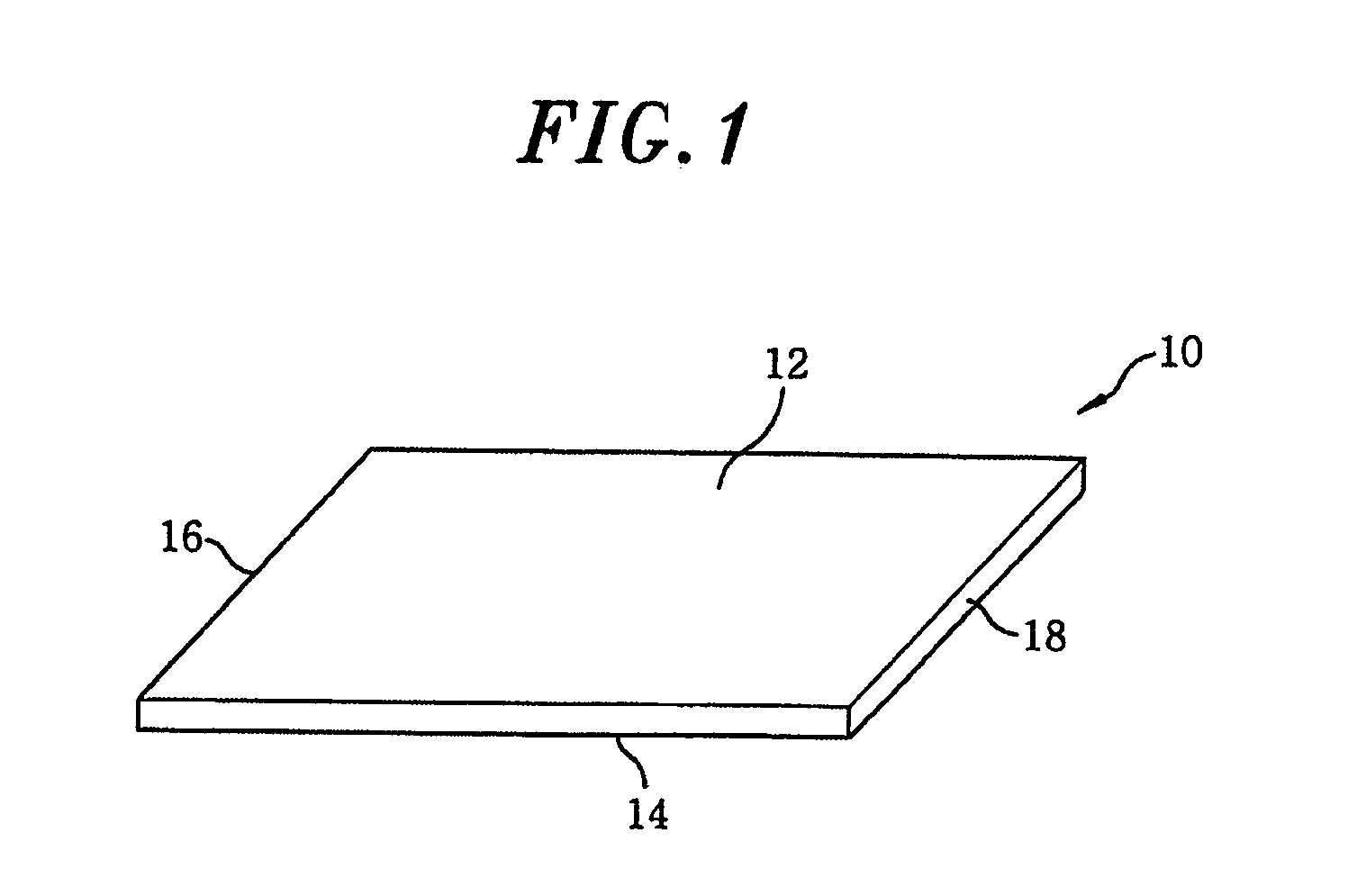
[0044]A single crystalline piezoelectric substrate (PMN-(0.3˜0.35)) PT having a thickness of about 0.4 mm to 0.5 mm and a size of about 25 mm to 22 mm×about 15 mm to 22 mm was prepared (see, FIG. 1). Then, on a first main surface 12, a second main surface 14, a first side surface 16 and a second side surface 18 of the first piezoelectric substrate 10, an electrode layer 12 of an electrical conductive material was deposited with the thickness ranging from about 1000 Å to 2200 Å by employing an electronic beam deposition method.

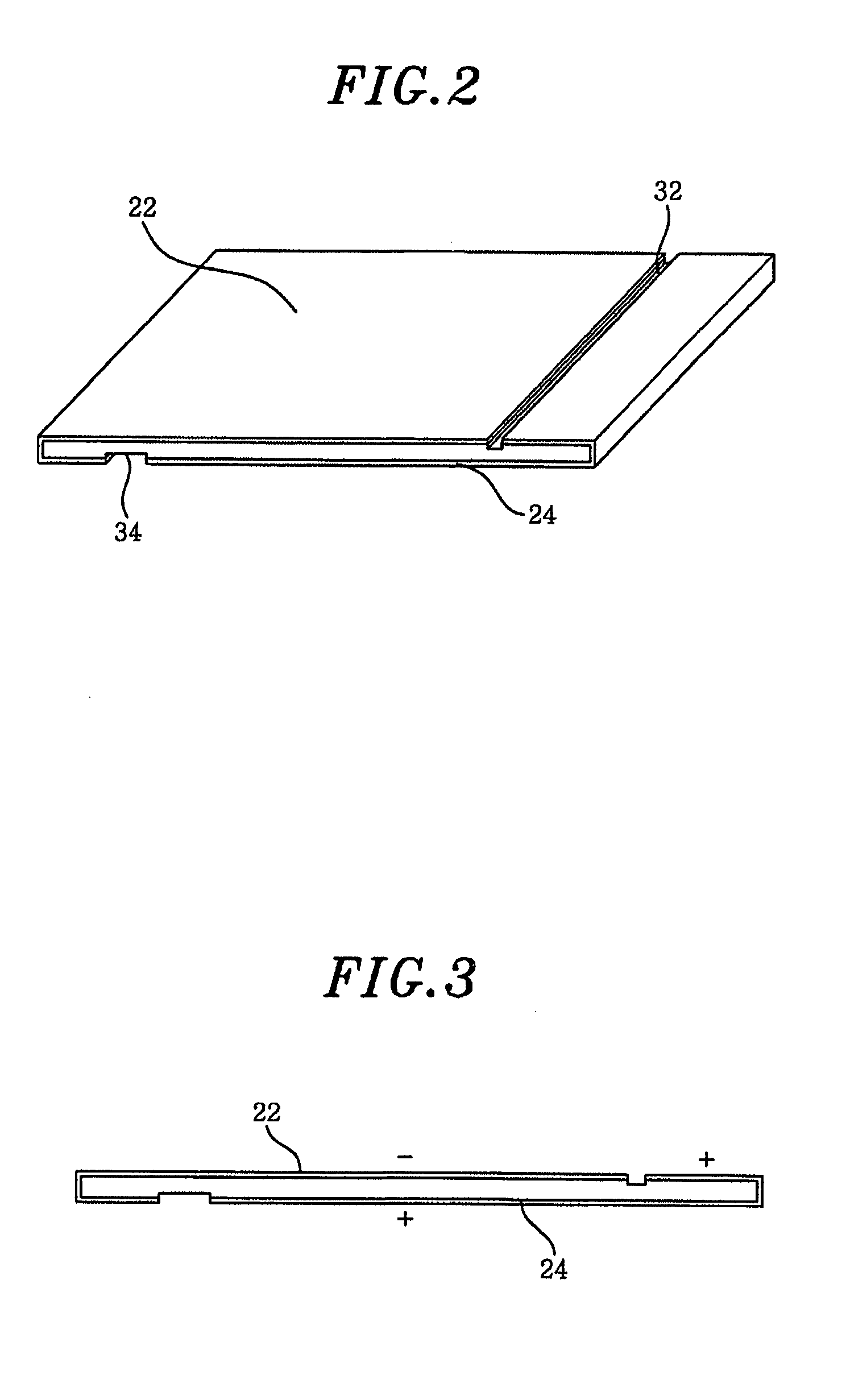
[0045]Then, another single crystalline piezoelectric substrate having electrodes formed thereon was fabricated by employing the same method as the above, to thereby obtain a second piezoelectric substrate 20.

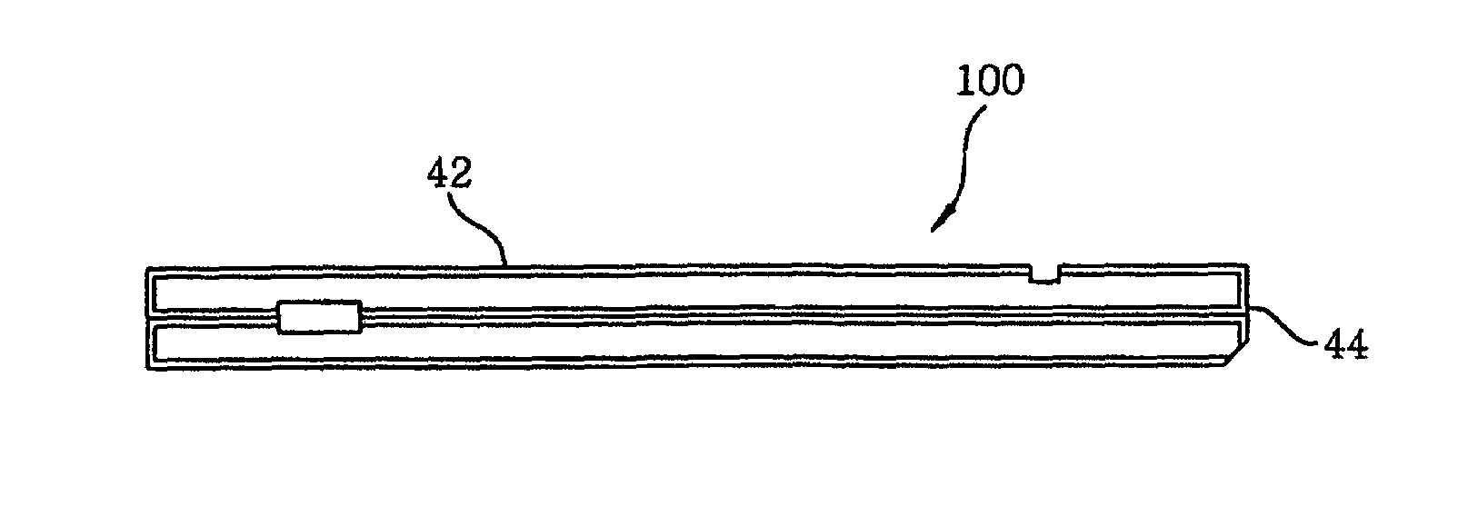
[0046]Subsequently, discontinuities 32 and 34 were formed in the electrode layer on the first and the second main surfac...

experimental example

[0051]Pulse-echo characteristics were inspected for each of the multilayer ultrasonic transducer according to the present invention; a PZT (Acuson P2-3AC available from Madison Co. Ltd. in Korea) single-layered transducer (Comparative Example 1) as similar as disclosed in U.S. Pat. No. 6,437,487; and a single-layered transducer of a PMN-(0.3˜0.35) PT system (Comparative Example 2), and the results were provided in the following Table 1 and in FIGS. 9 to 11.

[0052]

TABLE 1ComparativeComparativePreferredExample 1Example 2Embodiment(Single-layer(Single-layer(MultilayerPropertiesPZT)PMN-PT)PMN-PT)RelativeDB0+4.1+7.8SensitivityCentralMHz2.853.664.01Frequency −6 dB%60.2107.9101.0Bandwidth−22 dB%98.7134.7137.4Bandwidth

[0053]From the table 1, it can be found that the multilayer transducer in accordance with the present invention has a highly improved sensitivity and a larger bandwidth compared to the single-layered PZT or single-layered crystalline piezoelectric transducers.

[0054]Furthermore,...


PUM

PropertyMeasurementUnit
widthaaaaaaaaaa
widthaaaaaaaaaa
electrical impedanceaaaaaaaaaa

Abstract

A multilayer ultrasonic transducer includes a multilayer piezoelectric substrate assembly (100) laminated with a first and a second piezoelectric substrate on top of each other, and having a first electrode node (42) and a second electrode (44) node polarized with a primary electrode and a secondary electrode, respectively, a flexible printed circuit board coupled to the first electrode node, a backing block with a predetermined thickness surrounded by the flexible printed circuit board, a ground flexible printed circuit board coupled to the second electrode node, and an acoustic matching layer deposited on the multilayer piezoelectric substrate assembly.

Description

TECHNICAL FIELD[0001]The present invention relates to a multilayer ultrasonic transducer and a method for the manufacture thereof; and, more particularly, to a multilayer ultrasonic transducer with an improved vibration feature and a method for the manufacture thereof.BACKGROUND ART[0002]Ultrasonic transducers for medical imaging have many components, and pitches among the components are getting smaller. As the dimensions of the components in an ultrasonic transducer decrease, a mismatch of electrical impedance between an ultrasonic image diagnostic system the ultrasonic transducer and an ultrasonic image diagnostic system is rising as a serious problem yet to be solved.[0003]In general, electrical impedance of the components in an ultrasonic transducer ranges from 100 ohms to 500 ohms while electrical impedance of typical cables used to communicate between the ultrasonic transducer and the ultrasonic image diagnostic system ranges from 50 ohms to 85 ohms, exhibiting great differenc...

Claims


Application Information

Patent Timeline
Patent Type & Authority Patents(United States)
IPC IPC(8): H01L41/083A61B8/00H01L41/09H01L41/18H01L41/22H01L41/277H01L41/297H04R17/00H04R31/00
CPCB06B1/0611H01L41/0471H01L41/0475H01L41/27Y10T29/42Y10T29/49005H01L41/083H10N30/871H10N30/875H10N30/50H10N30/05A45D1/04A45D1/08H05B3/20A45D2001/002
Inventor RHIM, SUNG MINJUNG, HO
Owner HUMANSCAN
Why Eureka
Try Eureka