Power amplifier and multistage amplification circuit including same

a multi-stage amplification and power amplifier technology, applied in the direction of amplifiers, amplifiers with semiconductor devices only, amplifiers with semiconductor devices, etc., can solve the problem of difficult to restrain the gain variation of power amplifiers

Active Publication Date: 2009-08-11
SHARP KK
View PDF28 Cites 16 Cited by
  • Summary
  • Abstract
  • Description
  • Claims
  • Application Information

AI Technical Summary

Benefits of technology

[0018]The present invention, conceived in view of the problems, has an objective of providing a power amplifier having a gain which exhibits restrained dependence on temperature and control input voltage and also of providing a multistage amplification circuit including the power amplifier.

Problems solved by technology

Therefore, with this structure, it is still difficult to restrain gain variations in the power amplifier.

Method used


Image

  • Power amplifier and multistage amplification circuit including same
  • Power amplifier and multistage amplification circuit including same
  • Power amplifier and multistage amplification circuit including same

Examples


embodiment 1

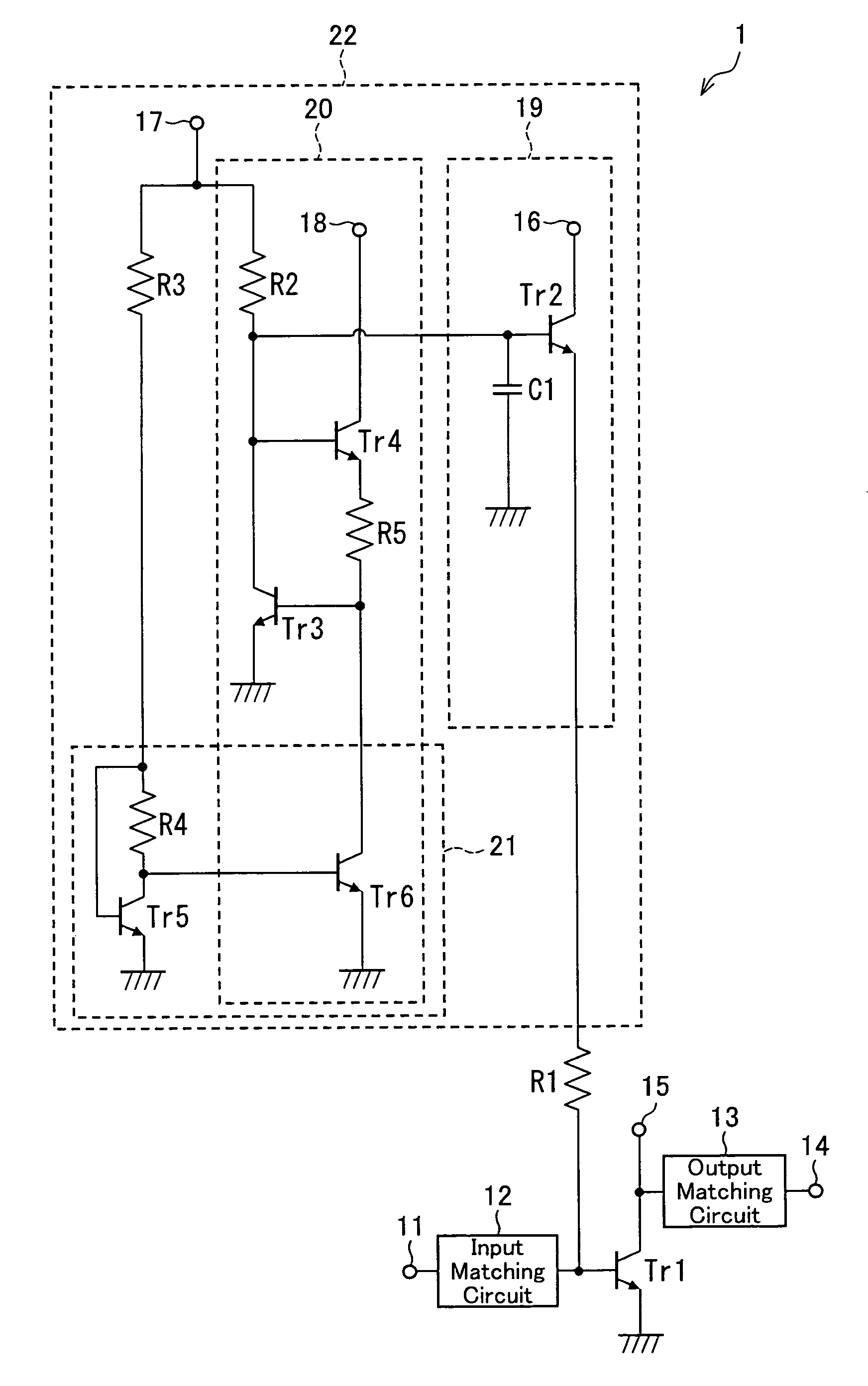
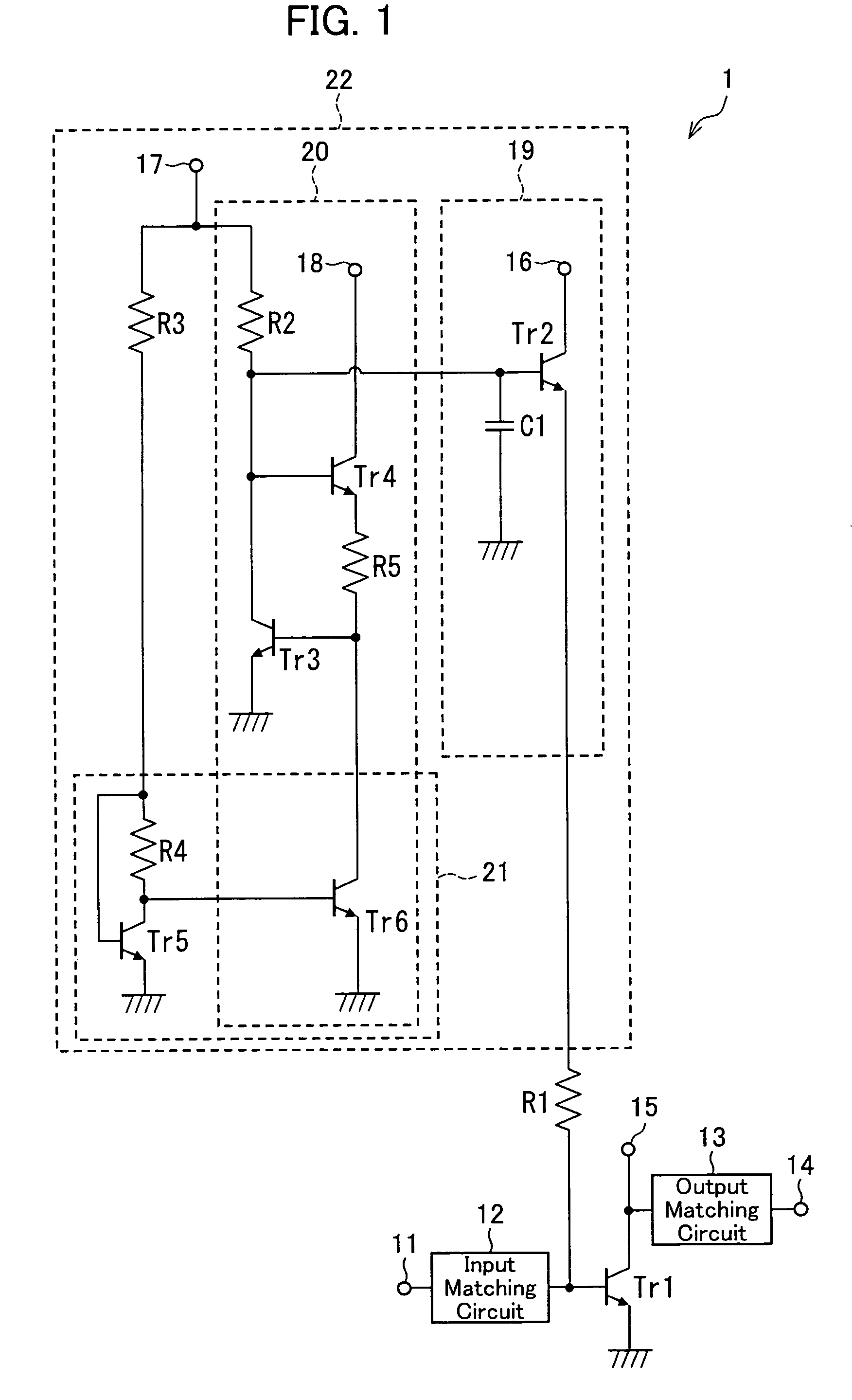
[0052]The following will describe an embodiment of the present invention in reference to FIGS. 1 to 17. FIG. 1 is a schematic circuit diagram of a power amplifier of the present embodiment.

[0053]As illustrated in FIG. 1, the power amplifier 1 of the present embodiment includes an amplification transistor (first amplification transistor) Tr1, an input matching circuit 12, an output matching circuit 13, a resistor R1, and a bias circuit (first bias circuit) 22. The amplification transistor Tr1 has its base connected to an input signal terminal 11 of the power amplifier 1 via the input matching circuit 12 and its collector connected to an output signal terminal 14 of the power amplifier 1 via the output matching circuit 13. In the power amplifier 1 thus configured, high frequency signals fed at the input signal terminal 11 are past through the input matching circuit 12, amplified by the amplification transistor Tr1, and then past through the output matching circuit 13 for output at the...

embodiment 2

[0121]The following will describe another embodiment of the present invention in reference to FIGS. 18 to 21. Those members of the present embodiment which have the same functions as members of embodiment 1 are indicated by the same reference numerals and description thereof is omitted.

[0122]FIG. 18 is a schematic circuit diagram of a power amplifier of the present embodiment. A power amplifier 3 of the present embodiment differs from the power amplifier 1 of embodiment 1 in that the VBE-controlled voltage source circuit 20b in the bias circuit (first bias circuit) 22b includes a resistor (fifth resistor) R6.

[0123]The bias circuit 22b in the power amplifier 3 includes a linear compensation circuit 19, a VBE-controlled voltage source circuit 20b, a Nagata current mirror circuit 21, a control input terminal 17, and a resistor R3. The VBE-controlled voltage source circuit 20b includes transistors Tr3, Tr4, Tr6 and resistors R2, R5, R6. The bias circuit 22b has similar functions to the ...

embodiment 3

[0136]The following will describe another embodiment of the present invention in reference to FIG. 22. Those members of the present embodiment which have the same functions as members of embodiments 1, 2 are indicated by the same reference numerals and description thereof is omitted.

[0137]FIG. 22 is a schematic circuit diagram of a power amplifier of the present embodiment. The power amplifier (multistage amplification circuit) 5 of the present embodiment differs from the power amplifiers 1 to 4 of embodiments 1, 2 in that the power amplifier 5 includes two amplification transistors connected to each other and adapted so that a bias circuit can produce a mirror current in each stage.

[0138]The power amplifier 5 includes, as illustrated in FIG. 22, an input matching circuit 12, an amplification transistor (first amplification transistor) Tr1a, an interstage matching circuit 23, another amplification transistor (third amplification transistor) Tr1b, an output matching circuit 13, and a...


PUM


Abstract

A bias circuit 22 in a power amplifier 1 is provided with a VBE-controlled voltage source circuit 20 and a Nagata current mirror circuit 21. The Nagata current mirror circuit 21 includes a transistor Tr5 and a transistor Tr6. The transistor Tr5 has its emitter grounded, its base connected to a control input terminal 17 via a resistor R3, and its collector connected to that base via a resistor R4. The transistor Tr6 has its emitter grounded, its base connected to the collector of the transistor Tr5, and its collector connected to the base of the transistor Tr3. The arrangement is capable of compensating both the temperature characteristics of the gain of the power amplifier 1 and the control input voltage characteristics of the gain of the power amplifier 1. In other words, the arrangement is capable of reducing the temperature dependence and control input voltage dependence of the gain of the power amplifier 1.

Description

[0001]This nonprovisional application claims priority under 35 U.S.C. § 119(a) on Patent Application No. 2007-023486 filed in Japan on Feb. 1, 2007, the entire contents of which are hereby incorporated by reference.FIELD OF THE INVENTION[0002]The present invention relates to power amplifiers with a bias circuit for compensating a temperature characteristic of the power amplifiers and also relates to multistage amplification circuits including such a power amplifier.BACKGROUND OF THE INVENTION[0003]Bipolar transistors are conventional, popular amplifying components for power amplifiers for amplifying, for example, signals. For example, in a bipolar transistor used as an amplifying component, the base-emitter ON voltage (VBE) drops at high temperatures. So, the collector current increases with a rise in ambient temperature if the bias voltage applied to the base is constant.[0004]To compensate this particular temperature characteristic to achieve stability of the power amplifier, the ...

Claims


Application Information

Patent Timeline
Patent Type & Authority Patents(United States)
IPC IPC(8): H03F3/04
CPCH03F1/302H03F3/211H03G1/04H03F2200/18H03F2200/411H03F2200/447H03F2200/318
Inventor ISHIMARU, YOSHITERUFURUKAWA, MOTOKO
Owner SHARP KK
Why Eureka
Try Eureka