Semiconductor integrated circuit, design support software system and automatic test pattern generation system

a technology of integrated circuits and software systems, applied in memory systems, error detection/correction, instruments, etc., can solve problems such as raising a problem of increasing costs

Active Publication Date: 2009-08-18
KK TOSHIBA
View PDF8 Cites 18 Cited by
  • Summary
  • Abstract
  • Description
  • Claims
  • Application Information

AI Technical Summary

Problems solved by technology

Further, some memory circuits have a memory having a redundant configuration for repairing a faulty cell.
In other words, a measure, such as to provide a pattern storage capacity to the tester for inputting the test pattern is necessitated, which storage capacity has to be sufficient for holding shift patterns corresponding to all the repair codes, thus raising a problem of increasing cost.

Method used


Image

  • Semiconductor integrated circuit, design support software system and automatic test pattern generation system
  • Semiconductor integrated circuit, design support software system and automatic test pattern generation system
  • Semiconductor integrated circuit, design support software system and automatic test pattern generation system

Examples


first embodiment

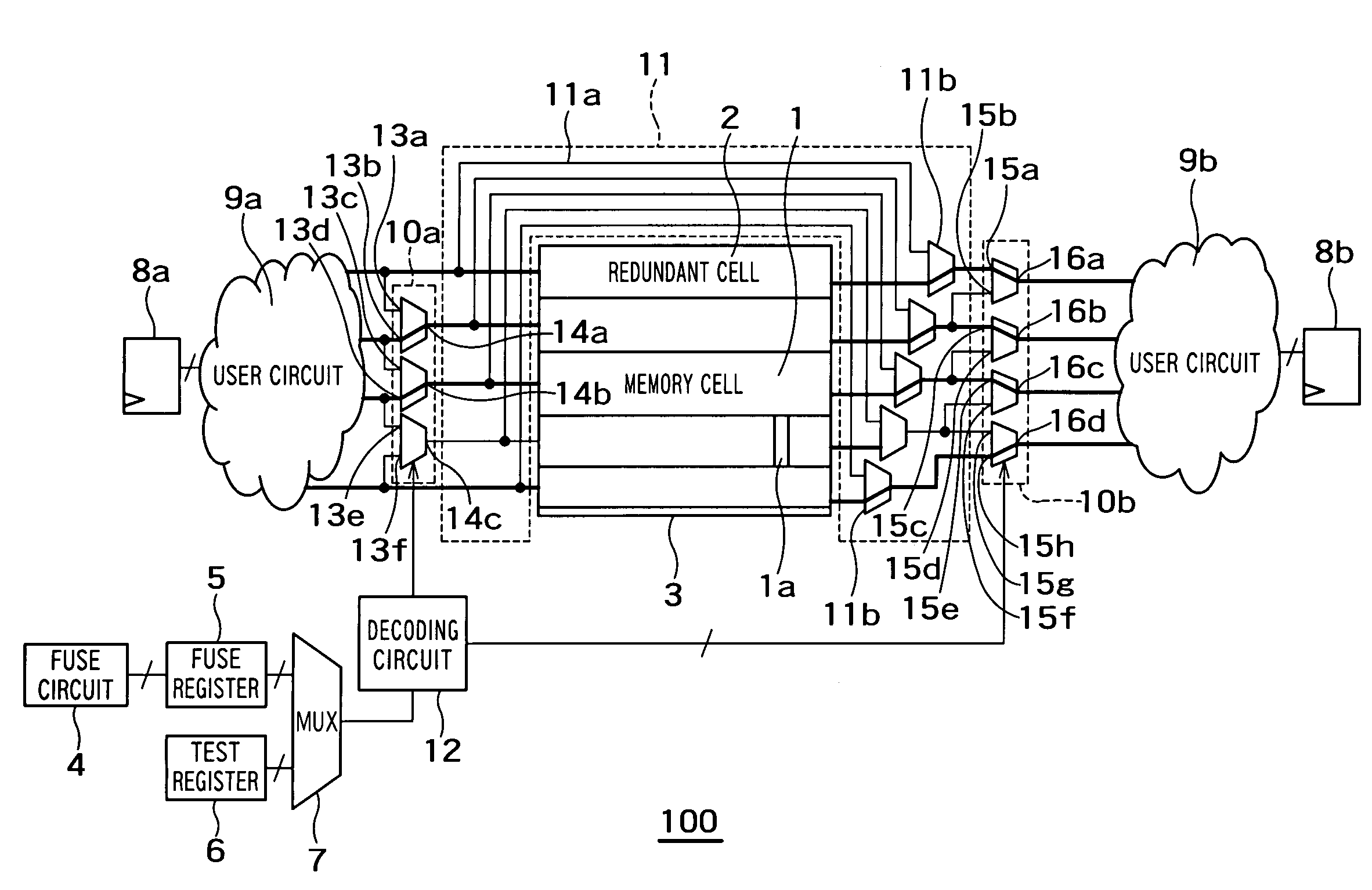
[0028]FIG. 1 is a block diagram illustrating a configuration of a principal part of a semiconductor integrated circuit according to a first embodiment of the present invention.

[0029]As shown in FIG. 1, a semiconductor integrated circuit 100 includes a memory circuit 3 having memory cells 1 and a redundant cell 2 for avoiding a faulty cell 1a among the memory cells 1, in which fault has occurred, to achieve repair; a fuse circuit 4 for determining a logic for repairing the memory circuit based on a repair code for avoiding the faulty cell la detected as a result of testing the memory circuit 3 and for using the redundant cell 2, and a fuse register 5, or a first register, which is controlled by output signals of the fuse circuit 4.

[0030]The semiconductor integrated circuit 100 further includes a stuck-at fault test register 6, or a second register, which is provided with a scan design for testing stuck-at faults, and has a test input and a test output; and a register selection circui...

second embodiment

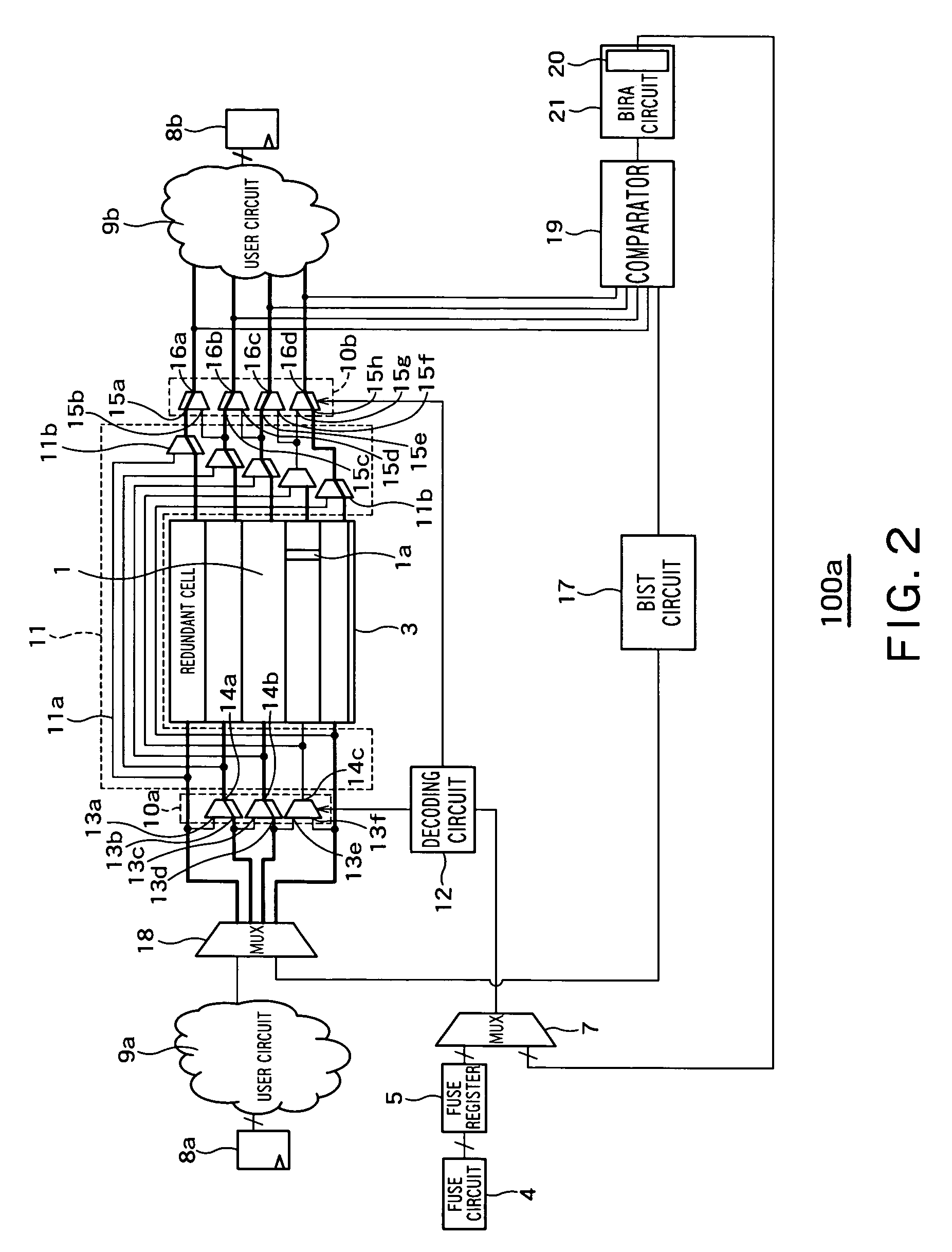
[0051]In the first embodiment, description has been provided on a configuration in which the stuck-at fault test register with scan design is separately provided in the semiconductor integrated circuit to test stuck-at faults.

[0052]In the present embodiment, in particular, description is provided on a configuration in which a register in a BIRA circuit is used as a stuck-at fault test register, the BIRA circuit producing a repair code based on a comparison result produced by a BIST circuit for testing a memory circuit.

[0053]FIG. 2 is a block diagram illustrating a configuration of a principal part of a semiconductor integrated circuit according to a second embodiment of the present invention. In the figure, the same references as in the first embodiment indicate the same components as in the first embodiment.

[0054]As shown in FIG. 2, a semiconductor integrated circuit 100a further includes a BIST (built-in self test) circuit 17 for outputting a test pattern for testing the memory ce...

third embodiment

[0063]In the first embodiment, description has been provided in detail on a configuration of the semiconductor integrated circuit.

[0064]In the present embodiment, description is provided, in particular, on a design support software system for supporting a test circuit design of the semiconductor integrated circuit.

[0065]FIG. 3 illustrates a design support software system according to the present embodiment. What is described here is the case where the design support software system produces a redundancy circuit file for the first embodiment, for incorporation into a net list of the semiconductor integrated circuit.

[0066]As shown in FIG. 3, a design support software system 200 includes a redundancy circuit producing portion 32 for producing a redundancy circuit file 31 based on an input from a redundant memory information file 30; and a circuit incorporation portion 37 for producing a second net list 36 in which redundancy circuits are incorporated based on inputs from the redundancy...


PUM


Abstract

A semiconductor integrated circuit has a memory circuit having memory cells, a first register, a second register, a register selection circuit having an input to which an output of the first register and an output of the second register are connected, a memory bypass circuit which is located between a first switching circuit and a second switching circuit, and connected to the inputs and the outputs of the memory circuit. The register selection circuit is switched to the output signals of the first register when performing testing by way of the memory circuit, and switched to output signals of the second register when performing testing by way of the memory bypass circuit.

Description

CROSS-REFERENCE TO RELATED APPLICATION[0001]This application is based upon and claims the benefit of priority from the prior Japanese Patent Application No. 2005-284429, filed on Sep. 29, 2005, the entire contents of which are incorporated herein by reference.BACKGROUND OF THE INVENTION[0002]1. Field of the Invention[0003]The present invention relates to a semiconductor integrated circuit for testing stuck-at faults and delay faults of a repair circuit, for example, in a memory having a redundant configuration and relates to a design support software system and an automatic test pattern generation system.[0004]2. Background Art[0005]Some techniques for detecting faults of devices in a manufacturing test use a BIST (built-in self test) circuit, for example, which tests a memory circuit set in a semiconductor integrated circuit.[0006]Methods for detecting faults in a memory circuit include, for example, a comparator-type BIST method in which comparison is made between written-in data ...

Claims


Application Information

Patent Timeline
Patent Type & Authority Patents(United States)
IPC IPC(8): G11C29/00
CPCG11C29/54G11C2029/3602G11C2029/0405
Inventor HASEGAWA, TETSUTOKUNAGA, CHIKAKO
Owner KK TOSHIBA
Why Eureka
Try Eureka