Organic electroluminescent display device and method of fabricating the same

a technology of organic electroluminescent display and organic el, which is applied in the direction of luminescent screens, discharge tubes, identification means, etc., can solve the problems of limited production yield of limited display size and high operating cost of passive matrix organic el display devices. achieve uniform image quality and uniform image quality

Active Publication Date: 2009-09-01
LG DISPLAY CO LTD
View PDF22 Cites 2 Cited by
  • Summary
  • Abstract
  • Description
  • Claims
  • Application Information

AI Technical Summary

Benefits of technology

[0018]An object of the present invention is to provide an organic EL display device having an absorbent element, thereby effectively removing moisture in the organic EL display device and increasing product life span.
[0020]Another object of the present invention is to provide an organic EL display device having uniform image quality.
[0021]Another object of the present invention is to provide a method of fabricating an organic EL display device having uniform image quality.

Problems solved by technology

While both the passive matrix organic EL display device and the active matrix organic EL display device have simple structures and are formed by a simple fabricating process, the passive matrix organic EL display device requires a relatively high amount of power to operate.
In addition, the display size of a passive matrix organic EL display device is limited by its structure.
Since the organic EL layer's yield is relatively low, the production yield of the organic EL display device is limited by the organic EL layer's yield.
For example, even when a TFT is properly fabricated, an organic EL display device can be determined to be unacceptable due to defects of the organic EL layer using a thin film of about 1000 Å thickness.
Accordingly, this limitation causes loss of materials and an increase in production costs.
However, the bottom emission-type organic EL display devices are not adequate for implementation in display devices that require high resolution due to the limitations of the increased aperture ratio.
However, since a cathode is commonly formed over the organic EL layer in the top emission-type organic EL display devices, material selection and light transmittance are limited such that light transmission efficiency is lowered.
For instance, if a thin film type passivation layer is formed to prevent a reduction of the light transmittance, the thin film type passivation layer may fail to prevent infiltration of exterior air into the device.

Method used


Image

  • Organic electroluminescent display device and method of fabricating the same
  • Organic electroluminescent display device and method of fabricating the same
  • Organic electroluminescent display device and method of fabricating the same

Examples


Embodiment Construction

[0034]Reference will now be made in detail to the preferred embodiments, examples of which are illustrated in the accompanying drawings.

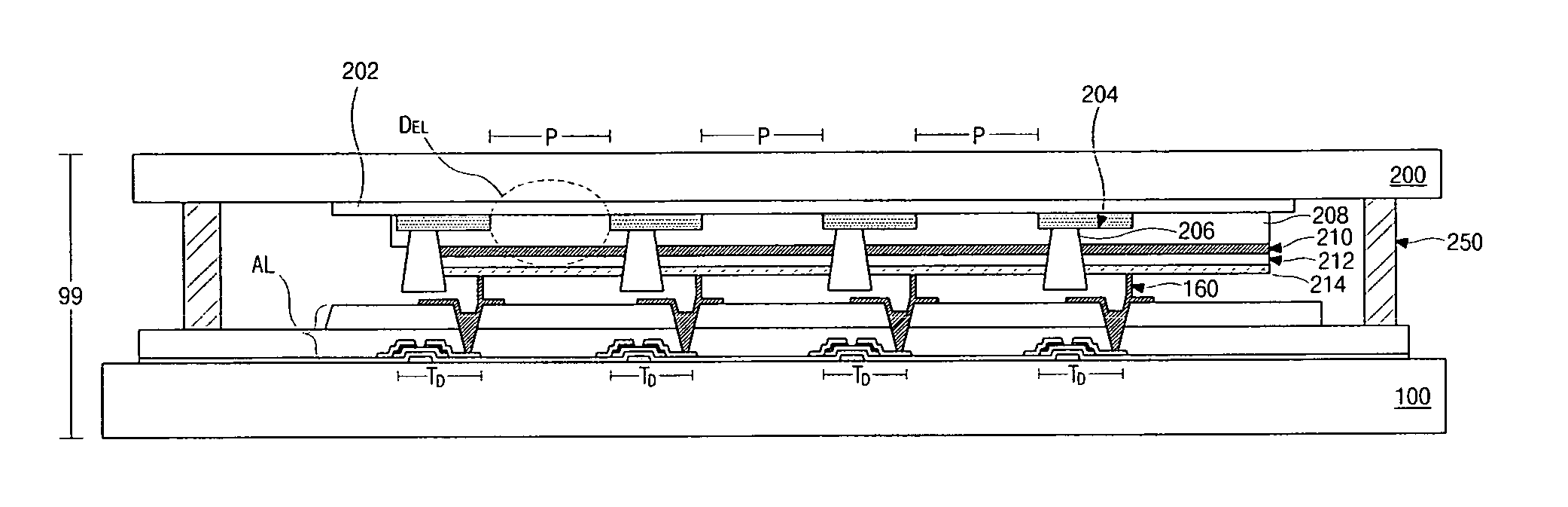
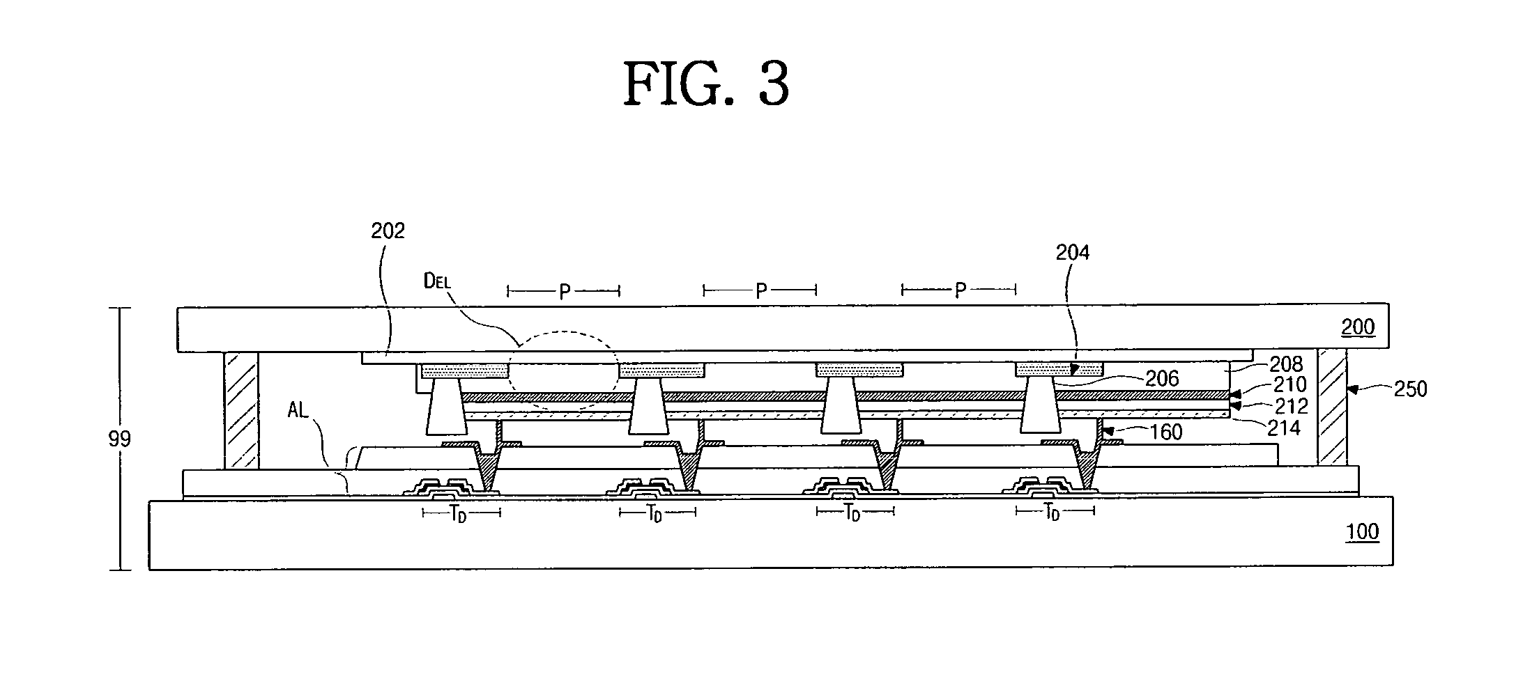
[0035]FIG. 3 is a schematic cross-sectional view of a dual panel type organic EL display device according to an embodiment of the present invention. In FIG. 3, an organic EL display device 99 includes a first substrate 100 and a second substrate 200 attached to each other by a sealant 250 with a predetermined space therebetween. An array element layer AL is formed on the first substrate 100, and an organic EL diode DEL is formed on the second substrate 200. The organic EL display device 99 includes a plurality of pixel regions P within a display region.

[0036]In particular, the array element layer AL includes a driving thin film transistor (TFT) TD in each of the pixel regions P. Although not shown, the array element layer AL additionally may include a scan line, a signal line and a power supply line intersected the scan line, a switching thin film t...


PUM


Abstract

An organic electroluminescent device includes first and second substrates spaced apart from each other, the first and second substrates including a pixel region, an array element layer on an inner surface of the first substrate, the array element layer including a switching element and a driving element connected to the switching element, an organic electroluminescent diode on an inner surface of the second substrate, an absorbent element on one of the array element layer and the organic electroluminescent diode, a protective layer on the absorbent element, and a connection electrode electrically connecting the array element layer and the organic electroluminescent diode.

Description

[0001]The present application claims the benefit of Korean Patent Application No. 2003-0099359 filed in Korea on Dec. 29, 2003, which is hereby incorporated by reference.BACKGROUND OF THE INVENTION[0002]1. Field of the Invention[0003]The present invention relates to a display device, and more particularly, to a dual panel type organic electroluminescent (EL) display device and a method of fabricating the same.[0004]2. Discussion of the Related Art[0005]An organic electroluminescent (EL) display device, which is a type of flat panel display, is a self-emission type display. In general, the organic EL display device emits light by injecting electrons from a cathode and holes from an anode into an emission layer, combining the electrons with the holes, generating an exciton, and transitioning the exciton from an excited state to a ground state. Accordingly, the organic EL display device does not require an additional light source and has a light weight, thin profile, and compact size.[...

Claims


Application Information

Patent Timeline
Patent Type & Authority Patents(United States)
IPC IPC(8): H01J1/62H01J9/00H05B33/04G09F9/00G09F9/30G09G3/30H01L27/32H01L51/50H01L51/52H05B33/02H05B33/10H05B33/12H05B33/14H05B33/22H05B33/26H05B44/00
CPCH01L51/5237H01L27/3251H01L27/3246H10K59/127H10K59/122H10K50/846H05B33/04
Inventor PARK, JAE-YONGKIM, KWAN-SOO
Owner LG DISPLAY CO LTD
Why Eureka
Try Eureka