Low voltage differential signaling drivers including branches with series resistors

a low voltage differential and signaling technology, applied in logic circuit coupling/interface arrangement, pulse technique, baseband system details, etc., can solve the problems of signal reflection and severe noise of the transmission unit tx of the first chip cpb>1/b>, and achieve low signal reflection, reduce the number of pins, and high operating speed

Active Publication Date: 2009-09-29
SAMSUNG ELECTRONICS CO LTD
View PDF10 Cites 36 Cited by
  • Summary
  • Abstract
  • Description
  • Claims
  • Application Information

AI Technical Summary

Benefits of technology

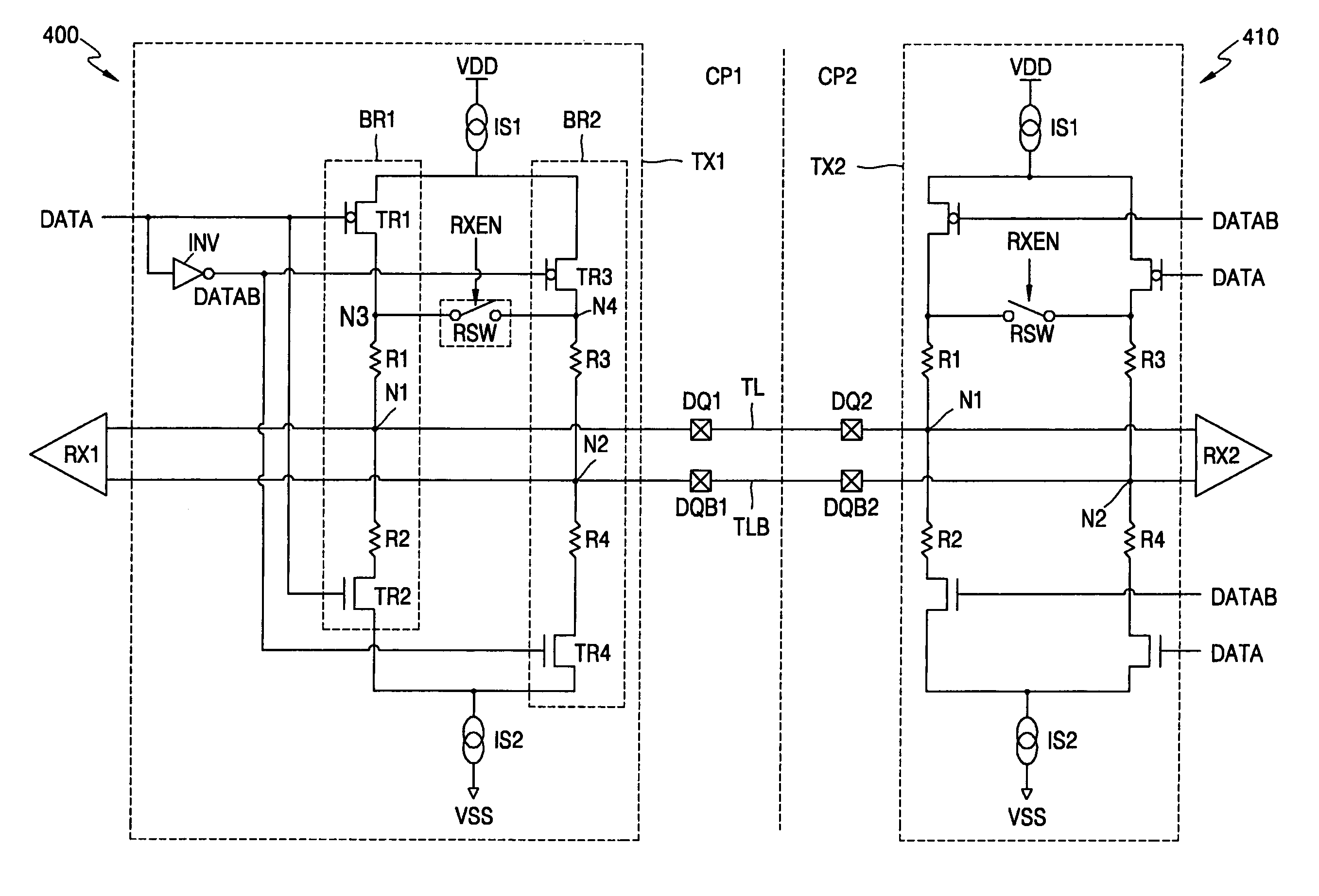
[0019]Exemplary embodiments of the present invention can provide low voltage differential signaling drivers which can minimize signal reflections by transmitting signals using terminal resistors installed in a transmission unit, can reduce the number of pins by half by using pins for both transmitting and receiving signals, and / or can achieve high operating speed while consuming less power.
[0021]Other embodiments of the present invention provide low voltage differential signaling drivers which receive data and transmit and receive differential signals via transmission lines. These low voltage differential signaling drivers include: first and second current sources, which are connected to a power supply voltage and a ground voltage, respectively; a first branch, which comprises at least two transistors connected to each other in series between the first and second current sources and a first node connected to one of the transmission lines; and a second branch, which comprises at least two transistors connected to each other at a second node in series between the first and second current sources and a second node connected to another of the transmission lines. The first branch further comprises resistors connected to each other in series between the transistors, which can reduce signal reflections caused by load resistance connected to the transmission lines, and the second branch further comprises resistors connected to each other in series between the transistors, which can reduce signal reflections caused by the load resistance connected to the transmission lines.
[0030]Other embodiments of the present invention provide low voltage differential signaling drivers. These low voltage differential signaling drivers include: a driving unit which is configured to output a pull-down signal having a first common mode voltage level and a pull-up signal having a second common mode voltage level in response to a control signal, a clock signal, and data; a transmission unit which is configured to output an output differential signal via transmission lines in response to the pull-up signal and the pull-down signal output from the driving unit; and a reception unit which is configured to receive an input differential signal via the transmission lines. In some embodiments, the transmission unit includes: first and second current sources, which are connected to a power supply voltage and a ground voltage, respectively; a first branch, which comprises at least two transistors connected to each other in series between the first and second current sources and a first node connected to one of the transmission lines; and a second branch, which comprises at least two transistors connected to each other in series between the first and second current sources and a second node connected to another of the transmission lines. The first branch also includes resistors connected to each other in series between the transistors, which can reduce signal reflections caused by load resistance connected to the transmission lines, and the second branch further comprises resistors connected to each other in series between the transistors, which can reduce signal reflections caused by the load resistance connected to the transmission lines. Other embodiments of transmission units including first and second branches also may be provided.

Problems solved by technology

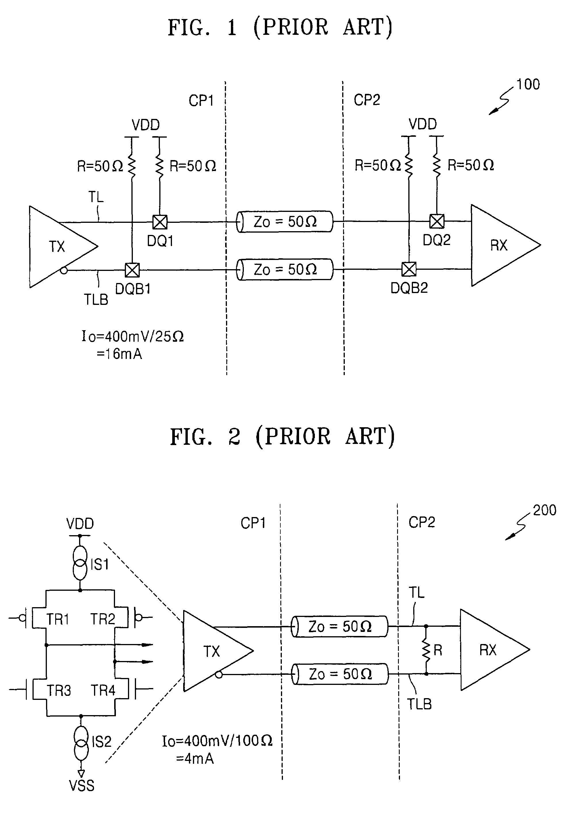
Thus, the transmission unit TX of the first chip CP1 may suffer from signal reflections and severe noise.

Method used


Image

  • Low voltage differential signaling drivers including branches with series resistors
  • Low voltage differential signaling drivers including branches with series resistors
  • Low voltage differential signaling drivers including branches with series resistors

Examples


Embodiment Construction

[0069]The present invention now will be described more fully hereinafter with reference to the accompanying drawings, in which illustrative embodiments of the invention are shown. However, this invention may be embodied in many different forms and should not be construed as limited to the embodiments set forth herein. Rather, these embodiments are provided so that this disclosure will be thorough and complete, and will fully convey the scope of the invention to those skilled in the art.

[0070]It will be understood that when an element is referred to as being “coupled”, “connected” or “responsive” to another element, it can be directly coupled, connected or responsive to the other element or intervening elements may also be present. In contrast, when an element is referred to as being “directly coupled”, “directly connected” or “directly responsive” to another element, there are no intervening elements present. Like numbers refer to like elements throughout. As used herein the term “a...


PUM


Abstract

A low voltage differential signal driver includes first and second current sources, a first branch and a second branch. The first branch includes at least two transistors and at least two resistors between them that are all connected in series between the first and second current sources, to define a first node between adjacent resistors that is configured to transmit and receive differential signals. The second branch also includes at least two transistors and at least two resistors between them that also are all connected in series between the first and second current sources, to define a second node between adjacent resistors that is also configured to transmit and receive differential signals.

Description

CROSS-REFERENCE TO RELATED PATENT APPLICATION[0001]This application claims the benefit under 35 USC § 119 of Korean Patent Application No. 10-2004-0107994, filed on Dec. 17, 2004, the disclosure of which is hereby incorporated herein by reference in its entirety as if set forth fully herein.FIELD OF THE INVENTION[0002]The present invention relates to driver circuits and methods, and more particularly to low voltage differential signaling drivers and associated methods.BACKGROUND OF THE INVENTION[0003]Various signal transmission methods for transmitting data between elements of one device or between two or more devices have been developed.[0004]FIG. 1 is a circuit diagram of a current mode logic (CML) system using a conventional signal transmission method. Specifically, FIG. 1 illustrates the transmission of a signal between a transmission unit TX of a first chip CP1 and a reception unit RX of a second chip CP2 via transmission lines TL and TLB. Referring to FIG. 1, output pads DQ1 a...

Claims


Application Information

Patent Timeline
Patent Type & Authority Patents(United States)
IPC IPC(8): H03K19/0175H03B1/00H03K3/00
CPCH04L5/16H04L25/0292H04L25/028H03K19/0175H03F3/45
Inventor KIM, JIN-HYUN
Owner SAMSUNG ELECTRONICS CO LTD
Why Eureka
Try Eureka