Bond pad for wafer and package for CMOS imager

a bond pad and imager technology, applied in the direction of electrical apparatus, semiconductor devices, semiconductor/solid-state device details, etc., can solve the problems of ineffective adversely affecting the functioning of bond pads and conventional electronics, and conventional crack stop and edge seals are not ordinarily adequate to protect chips

Inactive Publication Date: 2009-11-24
SMARTSENS TECH CAYMAN CO LTD
View PDF6 Cites 58 Cited by
  • Summary
  • Abstract
  • Description
  • Claims
  • Application Information

AI Technical Summary

Benefits of technology

[0016]Furthermore, pursuant to another feature with regard to protecting the Schott package, the through-via connects to the tungsten (W) contacts, which are connected to the device region by an M1 or higher metal layer. The through-via etch stops on the SiN layer, which is located on top of the Si. This SiN layer protects copper (Cu) and devices from contaminants, which are associated with the through-via manufacturing process. The edge seal protects the copper (Cu) and devices from contaminants at the edge of the chip.

Problems solved by technology

In essence, although this may be directed to various diverse components, said packaging arrangements, contamination and entry of moisture is encountered by the packages through either the rear or the side edges thereof, in which conventional crack stop and edge seals are ineffective in attempting to protect the chip when utilizing new packaging methods, such as those disclosed for devices as CMOS image sensors, including the known Schott package as described in the disclosure of “New Wafer-Level-Packaging Technology Using Silicon-Via-Contacts for Optical and Other Sensor Applications”, by Jürgen Leib and Michael Töpper in the 2004 Electronic Components and Technology Conference Proceedings, pages 843-847, and Shellcase package, as described in “An Innovative Approach to Wafer-lever MEMS packaging,” by D. Teomin, A. Badihi and G. Zilber (Shellcase Ltd., Manhat Technology Park) in Solid State Technology, V.45, n1; January 2002; pages 57-62.
As a result, the conventional crack stop and edge seal is not ordinarily adequate in protection of the chip when employing these new packaging arrangements and methods in the technology.
In the construction of other kinds of conventional devices, the crack stop and edge seals are also frequently inadequate to be able to preclude the entry of moisture and contaminating materials, which would adversely affect the functioning of the bond pads and the conventional electronics.

Method used


Image

  • Bond pad for wafer and package for CMOS imager
  • Bond pad for wafer and package for CMOS imager
  • Bond pad for wafer and package for CMOS imager

Examples


Embodiment Construction

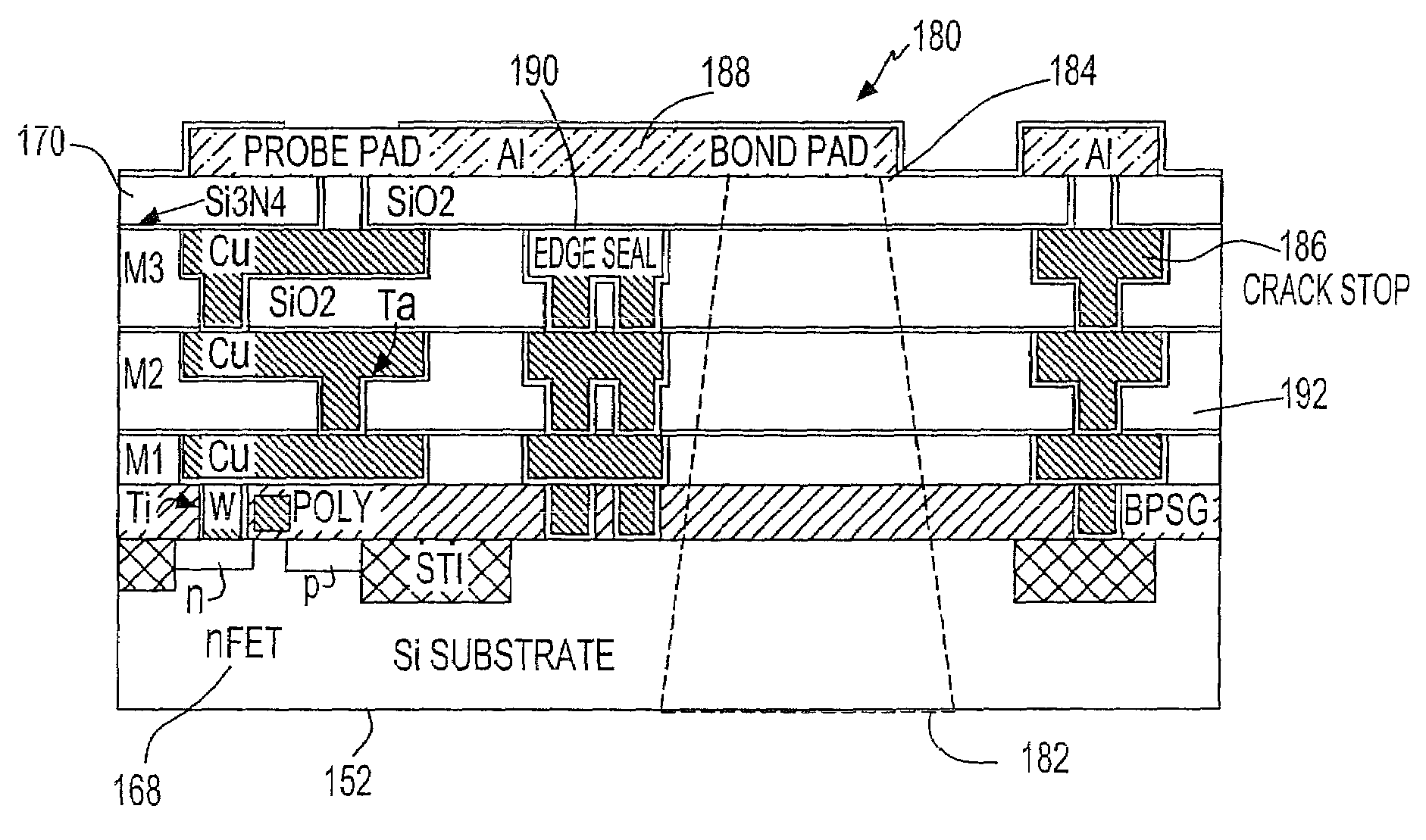
[0031]As disclosed in the above-mentioned copending application Ser. No. 10 / 904,677, the following electronic package structure is deemed to be of interest, as applied hereto:

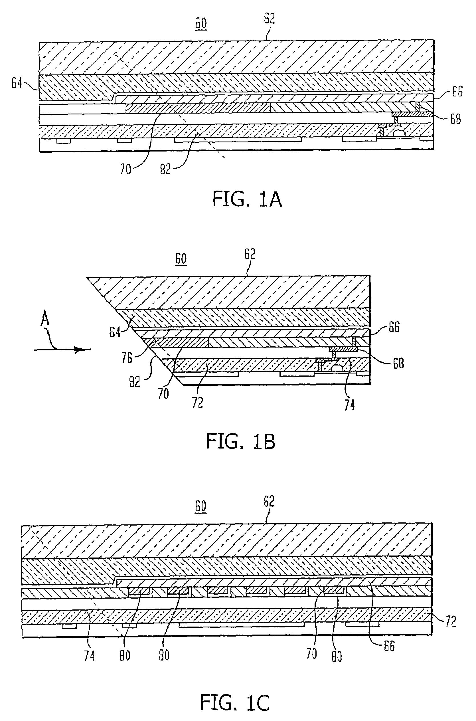
[0032]A first one of an electronic package embodiment (W+Al via bar, no additional masks) is shown in FIGS. 1A through 1C of the drawings.

[0033]Reverting in greater particularity to the drawings, and especially as exemplified in FIGS. 1A through 1C, there is diagrammatically shown in FIG. 1A a side view of an electronic package 60 in which a notch has been formed to expose the bond pads. Provided is a glass plate 62, the back surface thereof including a polymer layer 64, and along the edges at one side consisting of silicon dioxide or silicon nitrate, and the rear surface of which is contacted by an Al or aluminum bond pad 66. A via 68 is provided beneath the bond pad 66. Tungsten (W) via bars 68 are provided at one end of bond pad 66, to provide connection to the circuits. Tungsten (W) via bar 70 is provided b...


PUM


Abstract

An electronic packaging having at least one bond pad positioned on a chip for effectuating through-wafer connections to an integrated circuit. The electronic package is equipped with an edge seal between the bond pad region and an active circuit region, and includes a crack stop, which is adapted to protect the arrangement from the entry of deleterious moisture and combination into the active regions of the chip containing the bond pads.

Description

BACKGROUND OF THE INVENTION[0001]1. Field of the Invention[0002]The present invention relates to the provision of a bond pad for effecting through-wafer connections to an integrated circuit or electronic package, and wherein the bond pad includes a high surface area aluminum bond pad in order to resultingly obtain a highly reliable, low resistance connection between bond pads and electrical leads. In particular, the invention is directed to the addition of an edge seal between the bond pad region and an active circuit region, and includes a crack stop, which is adapted to protect the arrangement from the entry of deleterious moisture and combination into the active regions of the chip containing bond pads.[0003]In the current state-of-the-technology, through-wafer connections are frequently employed in the formation of advanced types of electronic packages, for instance, such as, but not limited to, 3D packaging, MEMS packaging, or CMOS imager packaging. In particular, the process w...

Claims


Application Information

Patent Timeline
Patent Type & Authority Patents(United States)
IPC IPC(8): H01L21/00
CPCH01L23/562H01L23/585H01L24/03H01L24/05H01L23/3114H01L23/485H01L2924/1461H01L2224/05553H01L2924/01072H01L2924/01047H01L2924/01024H01L2224/05624H01L2924/01013H01L2924/01014H01L2924/01022H01L2924/01027H01L2924/01029H01L2924/01033H01L2924/01046H01L2924/01073H01L2924/01074H01L2924/01078H01L2924/01079H01L2924/01082H01L2924/014H01L2924/14H01L2224/0558H01L2924/01023H01L2924/00014H01L2924/00H01L2224/45099
Inventor ADKISSON, JAMES W.GAMBINO, JEFFREY P.JAFFE, MARK D.RASSEL, RICHARD J.
Owner SMARTSENS TECH CAYMAN CO LTD
Why Eureka
Try Eureka