Clock aware placement

a technology of clock and placement, applied in the field of clock aware placement, can solve the problems of large number of cells, difficult to achieve the effect of sacrificing timing requirements, and requiring complicated connections between cells

Inactive Publication Date: 2009-11-24
GLOBALFOUNDRIES INC
View PDF4 Cites 26 Cited by
  • Summary
  • Abstract
  • Description
  • Claims
  • Application Information

AI Technical Summary

Benefits of technology

[0011]It is therefore one object of the present invention to provide an improved placement method for designing the layout of an integrated circuit which takes the clock network into consideration and places sinks belonging to the same clock domain closer without sacrificing timing requirements.
[0012]It is another object of the present invention to provide such a method which does not impose unnecessary design constraints during placement yet can be efficiently carried out on a data processing system.
[0013]It is still another object of the present invention to provide a method for designing the layout of latches in a common clock domain which may advantageously utilize features of existing placement techniques such as quadratic placement.

Problems solved by technology

An IC may include a very large number of cells and require complicated connections between the cells.
Due to the large number of components and the details required by the fabrication process for very large scale integrated (VLSI) devices, physical design is not practical without the aid of computers.
While these techniques provide adequate placement of cells with regard to their data interconnections, there is an additional challenge for the designer in constructing a clock network for the cells and this challenge is becoming more difficult with the latest technologies like low-power, 65-nanometer integrated circuits. FIG. 1 illustrates a typical clock tree for a net of clock sinks such as latches 2 in a common clock domain that have been placed using conventional techniques.
Placement algorithms have a tendency to spread out the latches, creating a relatively large clock domain size which is undesirable since a larger clock domain can result in increased power consumption and lead to problems caused by variations in the delays to various clock sinks of paths originating at source 4.
This approach, however, is cumbersome and cannot produce optimal results due to overly restrictive constraints.
It can also be difficult to predict where to place the domains.
An alternative approach creates an artificial net connecting all latches in the same domain, but it is difficult to control the degree of attraction imposed by the artificial net which leads to poor wirelength, congestion and timing.
While this method provides some optimization of clock power, it is hard to properly represent clock tree structures in placement engines which leads to an undue amount of runtime overhead.

Method used


Image

  • Clock aware placement
  • Clock aware placement
  • Clock aware placement

Examples


Embodiment Construction

)

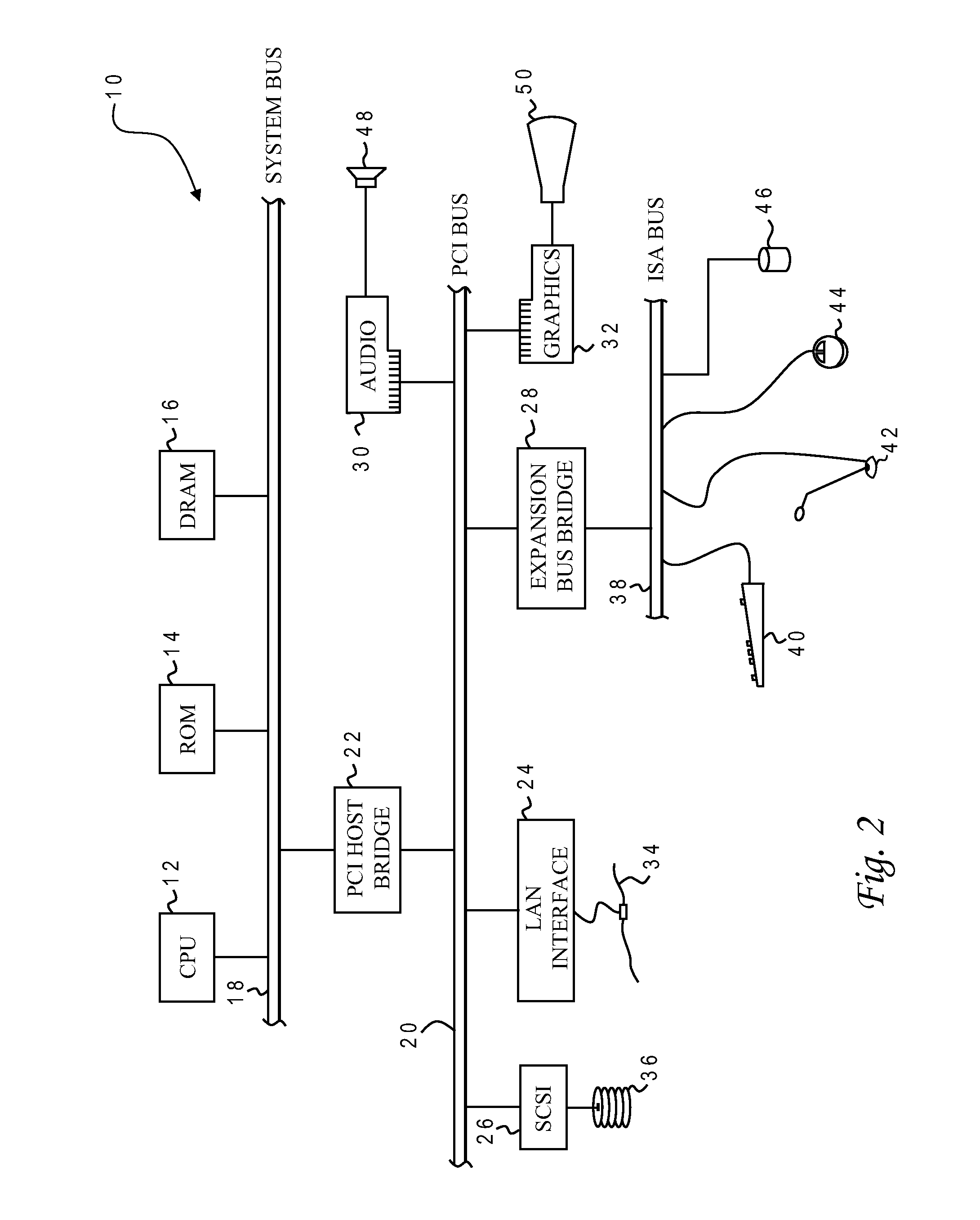
[0026]With reference now to the figures, and in particular with reference to FIG. 2, there is depicted one embodiment 10 of a computer system programmed to carry out computer-aided design of an integrated circuit in accordance with one implementation of the present invention. System 10 includes a central processing unit (CPU) 12 which carries out program instructions, firmware or read-only memory (ROM) 14 which stores the system's basic input / output logic, and a dynamic random access memory (DRAM) 16 which temporarily stores program instructions and operand data used by CPU 12. CPU 12, ROM 14 and DRAM 16 are all connected to a system bus 18. There may be additional structures in the memory hierarchy which are not depicted, such as on-board (L1) and second-level (L2) caches. In high performance implementations, system 10 may include multiple CPUs and a distributed system memory.

[0027]CPU 12, ROM 14 and DRAM 16 are also coupled to a peripheral component interconnect (PCI) local bus 2...


PUM


Abstract

The layout of latches in a common clock domain is efficiently optimized to shrink the physical size of the domain while maintaining timing requirements. The latches are placed in a first layout preferably using quadratic placement, and a star object is built representing an interim clock structure. The latches are weighted based on wire distance from a source of the star object, and then re-placed using the weighting. The weighted placement and repartitioning may be iteratively repeated until a target number of bins is reached. The boundary of the latches in the final global placement is used to define a movebound for further detailed placement.

Description

BACKGROUND OF THE INVENTION[0001]1. Field of the Invention[0002]The present invention generally relates to the fabrication and design of semiconductor chips and integrated circuits, and more particularly to a method of designing the physical layout (placement) of latches in a net having a common clock domain.[0003]2. Description of the Related Art[0004]Integrated circuits are used for a wide variety of electronic applications, from simple devices such as wristwatches to the most complex computer systems. A microelectronic integrated circuit (IC) chip can generally be thought of as a collection of logic cells with electrical interconnections between the cells, formed on a semiconductor substrate (e.g., silicon). An IC may include a very large number of cells and require complicated connections between the cells. A cell is a group of one or more circuit elements such as transistors, capacitors, resistors, inductors, and other basic circuit elements grouped to perform a logic function....

Claims


Application Information

Patent Timeline
Patent Type & Authority Patents(United States)
IPC IPC(8): G06F17/50
CPCG06F17/5072G06F30/392
Inventor ALPERT, CHARLES J.HATHAWAY, DAVID J.MIGATZ, WILLIAM R.NAM, GI-JOONREN, HAOXINGVILLARRUBIA, PAUL G.
Owner GLOBALFOUNDRIES INC
Why Eureka
Try Eureka