Latch Placement for High Performance and Low Power Circuits

a low-power, high-performance technology, applied in the direction of computer aided design, program control, instruments, etc., can solve the problems of large number of cells, difficult computer-aided physical design, and complicated connections between cells, etc., to achieve the effect of sacrificing timing requirements

Active Publication Date: 2008-06-19
GLOBALFOUNDRIES US INC
View PDF6 Cites 44 Cited by
  • Summary
  • Abstract
  • Description
  • Claims
  • Application Information

AI Technical Summary

Benefits of technology

[0013]It is therefore one object of the present invention to provide an improved placement method for designing the layout of an integrated circuit which takes the clock network into consideration and places latches belonging to different clock domains closer to their corresponding local clock buffer without sacrificing timing requirements.

Problems solved by technology

An IC may include a very large number of cells and require complicated connections between the cells.
Due to the large number of components and the details required by the fabrication process for very large scale integrated (VLSI) devices, physical design is not practical without the aid of computers.
While these techniques provide adequate placement of cells with regard to their data interconnections, there is an additional challenge for the designer in constructing a clock network for the cells and this challenge is becoming more difficult with the latest technologies like low-power, 65-nanometer integrated circuits.
Low power circuits (e.g., around 20 watts or less for microprocessor chips) are becoming more prevalent due to power consumption problems.
In particular, power dissipation has become a limiting factor for the yield of high-performance circuit designs (operating at frequencies around 1 gigahertz or more) with deep submicron technology.
The resulting LCB-latch structure is very large relative to other circuit elements involved in the placement process and greatly impacts the timing of the S circuit.
While this process has some advantages relative to the clock network, such restrictions seriously affect the flexibility of a placer and can often produce poor logic placement.

Method used


Image

  • Latch Placement for High Performance and Low Power Circuits
  • Latch Placement for High Performance and Low Power Circuits
  • Latch Placement for High Performance and Low Power Circuits

Examples


Embodiment Construction

)

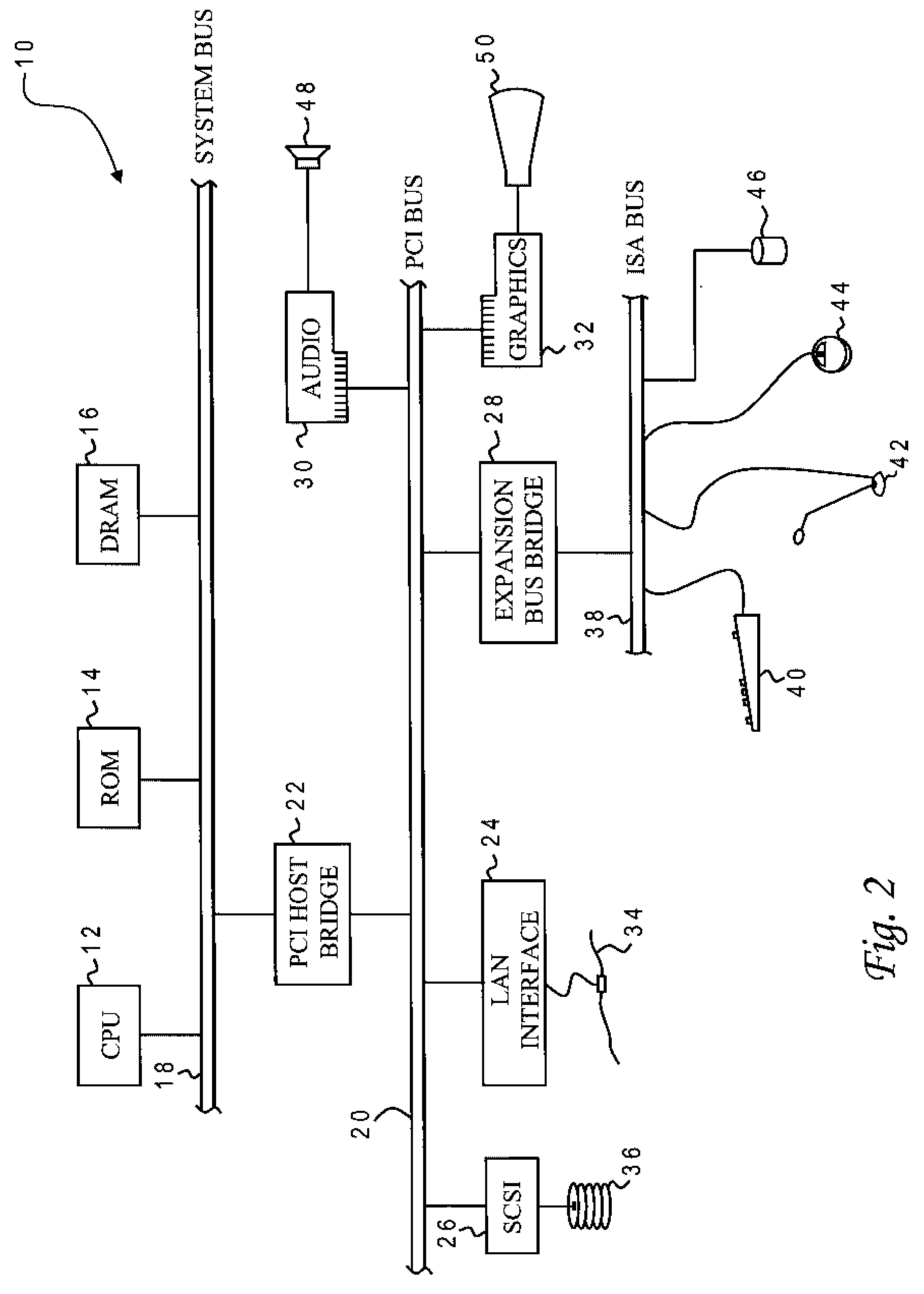
[0024]With reference now to the figures, and in particular with reference to FIG. 2, there is depicted one embodiment 10 of a computer system programmed to carry out computer-aided design of an integrated circuit in accordance with one implementation of the present invention. System 10 includes a central processing unit (CPU) 12 which carries out program instructions, firmware or read-only memory (ROM) 14 which stores the system's basic input / output logic, and a dynamic random access memory (DRAM) 16 which temporarily stores program instructions and operand data used by CPU 12. CPU 12, ROM 14 and DRAM 16 are all connected to a system bus 18. There may be additional structures in the memory hierarchy which are not depicted, such as on-board (L1) and second-level (L2) caches. In high performance implementations, system 10 may include multiple CPUs and a distributed system memory.

[0025]CPU 12, ROM 14 and DRAM 16 are also coupled to a peripheral component interconnect (PCI) local bus 2...


PUM


Abstract

A novel iterative latch placement scheme wherein the latches are gradually pulled by increasing attraction force until they are eventually placed next to a clock distribution structure such as a local clock buffer (LCB). During the iterations, timing optimizations such as gate sizing and re-buffering are invoked in order to keep the timing estimation accurate. By applying the iterative clock net weighting adjustment, the present invention allows tighter interaction between logic placement and clock placement which leads to higher quality timing and significant power savings.

Description

BACKGROUND OF THE INVENTION[0001]1. Field of the Invention[0002]The present invention generally relates to the fabrication and design of semiconductor chips and integrated circuits, and more particularly to a method of designing the physical layout (placement) of latches and other logic cells which receive clock signals from a clock distribution structure such as a local clock buffer.[0003]2. Description of the Related Art[0004]Integrated circuits are used for a wide variety of electronic applications, from simple devices such as wristwatches to the most complex computer systems. A microelectronic integrated circuit (IC) chip can generally be thought of as a collection of logic cells with electrical interconnections between the cells, formed on a semiconductor substrate (e.g., silicon). An IC may include a very large number of cells and require complicated connections between the cells. A cell is a group of one or more circuit elements such as transistors, capacitors, resistors, ind...

Claims


Application Information

Patent Timeline
Patent Type & Authority Applications(United States)
IPC IPC(8): G06F17/50
CPCG06F17/5072G06F30/392
Inventor ALPERT, CHARLES J.RAMJI, SHYAMSZE, CHIN NGAIVILLARRUBIA, PAUL G
Owner GLOBALFOUNDRIES US INC
Why Eureka
Try Eureka