Power MOS device with improved gate charge performance

a power mos and gate charge technology, applied in the field of field-effect transistors, can solve the problems of increasing the gate charge adverse effect, increasing the failure rate of transistors subject to higher gate charge, and difficult to achieve the alignment of terrace oxid

Inactive Publication Date: 2009-12-01
SEMICON COMPONENTS IND LLC
View PDF353 Cites 61 Cited by
  • Summary
  • Abstract
  • Description
  • Claims
  • Application Information

AI Technical Summary

Problems solved by technology

Increasing the gate charge has adverse effects.
Further, the failure rate of transistors subject to higher gate charge is increased.
First, for planar DMOS transistors, alignment of the terrace oxide is difficult to achieve, and adds significantly to the costs of manufacturing the devices.
Being easily misaligned, transistors formed with a terrace oxide have substantially lower yields.
The difficulty with which to build a non-uniform dielectric layer exists in trench DMOS structures as well.

Method used


Image

  • Power MOS device with improved gate charge performance
  • Power MOS device with improved gate charge performance
  • Power MOS device with improved gate charge performance

Examples


Embodiment Construction

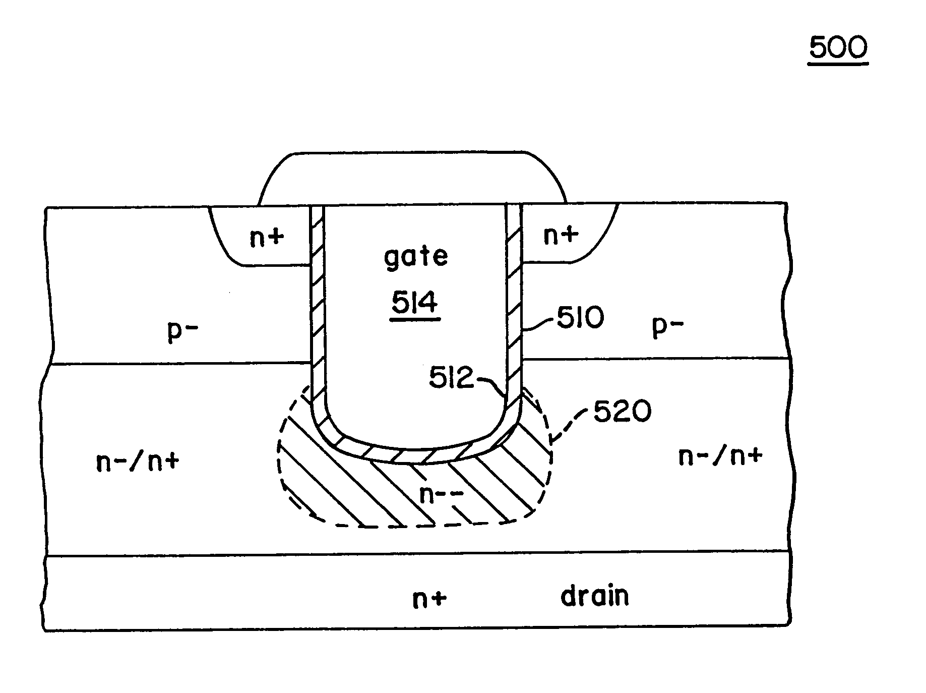
[0028]The present invention provides a composite gate structure and methods of manufacture. The composite gate structure lowers gate to drain overlap capacitance and enhances switching speed and efficiency.

[0029]FIG. 5 is a simplified cross section of a trench DMOS transistor 300 according to an embodiment of the present invention. This example illustrates an n− channel device, however, it is understood that the invention could be applied to an p− channel device. The DMOS transistor is fabricated on an n+ silicon substrate 320 that serves as the drain of the DMOS transistor. An n− epitaxial layer 325 is grown on the substrate. A p− channel region 332 and a p+ body region 305 are formed over the n− epitaxial layer, which is considered part of the “substrate” for purposes of this description. The p− channel region and p+ body region are formed by implanting and diffusing dopants of a p-type conductivity.

[0030]A trench 310 is formed into the substrate to a predetermined depth, extendin...


PUM


Abstract

A double-diffused metal-oxide-semiconductor (“DMOS”) field-effect transistor with an improved gate structure. The gate structure includes a first portion of a first conductivity type for creating electron flow from the source to the drain when a charge is applied to the gate. The gate structure includes a second portion of a second conductivity type having a polarity that is opposite a polarity of the first conductivity type, for decreasing a capacitance charge under the gate. A second structure for decreasing a capacitance under the gate includes an implant region in the semiconductor substrate between a channel region, where the implant region is doped to have a conductivity opposite the channel region.

Description

CROSS-REFERENCES TO RELATED APPLICATIONS[0001]This application is a continuation of U.S. patent application Ser. No. 10 / 391,126, filed on Mar. 17, 2003, which is a continuation of U.S. patent application Ser. No. 10 / 219,603, filed on Aug. 14, 2002, now U.S. Pat. No. 6,534,825, which is a division of U.S. patent application Ser. No. 09 / 468,269 filed on Dec. 20, 1999, now U.S. Pat. No. 6,461,918, which disclosures are incorporated herein by reference in their entirety for all purposes.BACKGROUND OF THE INVENTION[0002]The present invention relates to field-effect transistors, in particular double-diffused metal-oxide-semiconductor (“DMOS”) transistors, and their method of manufacture.[0003]A DMOS transistor is a type of field-effect transistor (“FET”) that can be used as a power transistor, that is, a transistor that is used to switch or control relatively large amounts of electrical power compared to a transistor that might be used in a logic circuit application. Power transistors mig...

Claims


Application Information

Patent Timeline
Patent Type & Authority Patents(United States)
IPC IPC(8): H01L21/8238H01L21/336H01L29/08H01L29/49H01L29/78
CPCH01L29/0878H01L29/4236H01L29/7813H01L29/4983H01L29/7802H01L29/4916H01L29/0847H01L29/42376H01L29/4933
Inventor CALAFUT, DANIEL S.
Owner SEMICON COMPONENTS IND LLC
Why Eureka
Try Eureka