Semiconductor structure

a technology of semiconductors and components, applied in the direction of burglar alarm mechanical actuation, burglar alarm by hand-portable objects removal, instruments, etc., can solve the problems of low quality factor parametrics, no longer have an effect, and approach can only be poorly implemented, so as to improve the characteristics

Active Publication Date: 2009-12-15
ATMEL CORP
View PDF22 Cites 4 Cited by
  • Summary
  • Abstract
  • Description
  • Claims
  • Application Information

AI Technical Summary

Benefits of technology

[0010]It is therefore an object of the present invention to provide a semiconductor structure, in particular for HF applications, which possesses further improved characteristics with respect to the effects of parasitic circuit components and which is also compatible in terms of its circuit layout with novel assembly methods for transponder or sensor ICs, especially methods using flip-chip technology.
[0013]In the course of a particularly preferred further development of the invention, the semiconductor structure created is characterized in that the first electrically conductive layer is formed by a receiving device of the semiconductor structure for electromagnetic waves, in particular an antenna of the transponder or remote sensor. In other words, the first capacitor of one / each stage of an RSSI or power supply rectifier is formed by the antenna and a first layer of the IC. Such an arrangement is extremely compact and economical to implement; moreover, the parasitic capacitance of the coupling capacitors is further reduced in this way.
[0015]For HF applications, the above-mentioned rectifier or RSSI circuits can use Schottky diodes, which in themselves have only a very small parasitic capacitance value as a result of negligible charge storage in the forward-biased state. To this end, a further embodiment of the inventive semiconductor structure has at least one first layer with metallic properties, which is arranged in a junction region between the dielectric layer and the first zone below the second electrically conductive layer and is electrically connected to the latter. It is thus possible within the scope of the invention to place the Schottky diodes directly under the pad and the first coupling capacitor, which in turn makes it possible to reduce the parasitic connections and the parasitic area of the “pad capacitor.”

Problems solved by technology

However, there also exists the possibility of providing parasitics with the lowest possible quality factor, so they no longer have an effect.
This approach can only be poorly implemented, however, especially in ICs with small dimensions, since implementing large resistors with low quality factors results in a corresponding need for space that is not available in many IC architectures and is thus cost-intensive.

Method used


Image

  • Semiconductor structure
  • Semiconductor structure
  • Semiconductor structure

Examples


Embodiment Construction

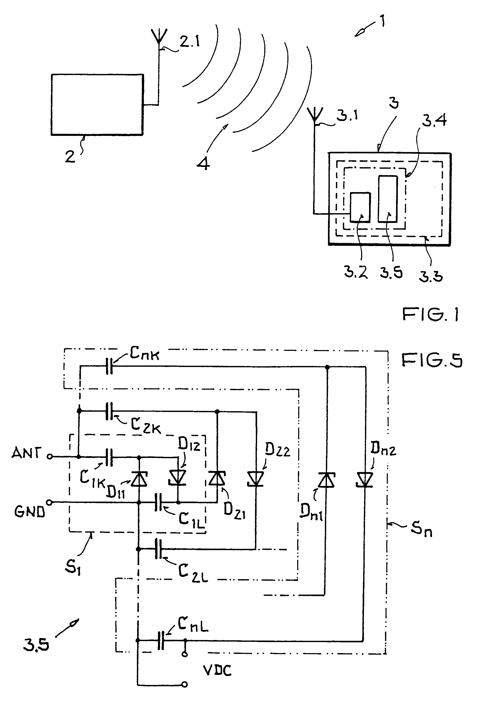
[0028]FIG. 1 shows a simplified, schematic representation of an RFID system 1 with a base station 2 and a passive transponder or remote sensor 3 that is supplied with electrical energy by an HF electromagnetic field 4 generated by the base station 2 and transmitted by a transmitting device 2.1 of the base station 2.

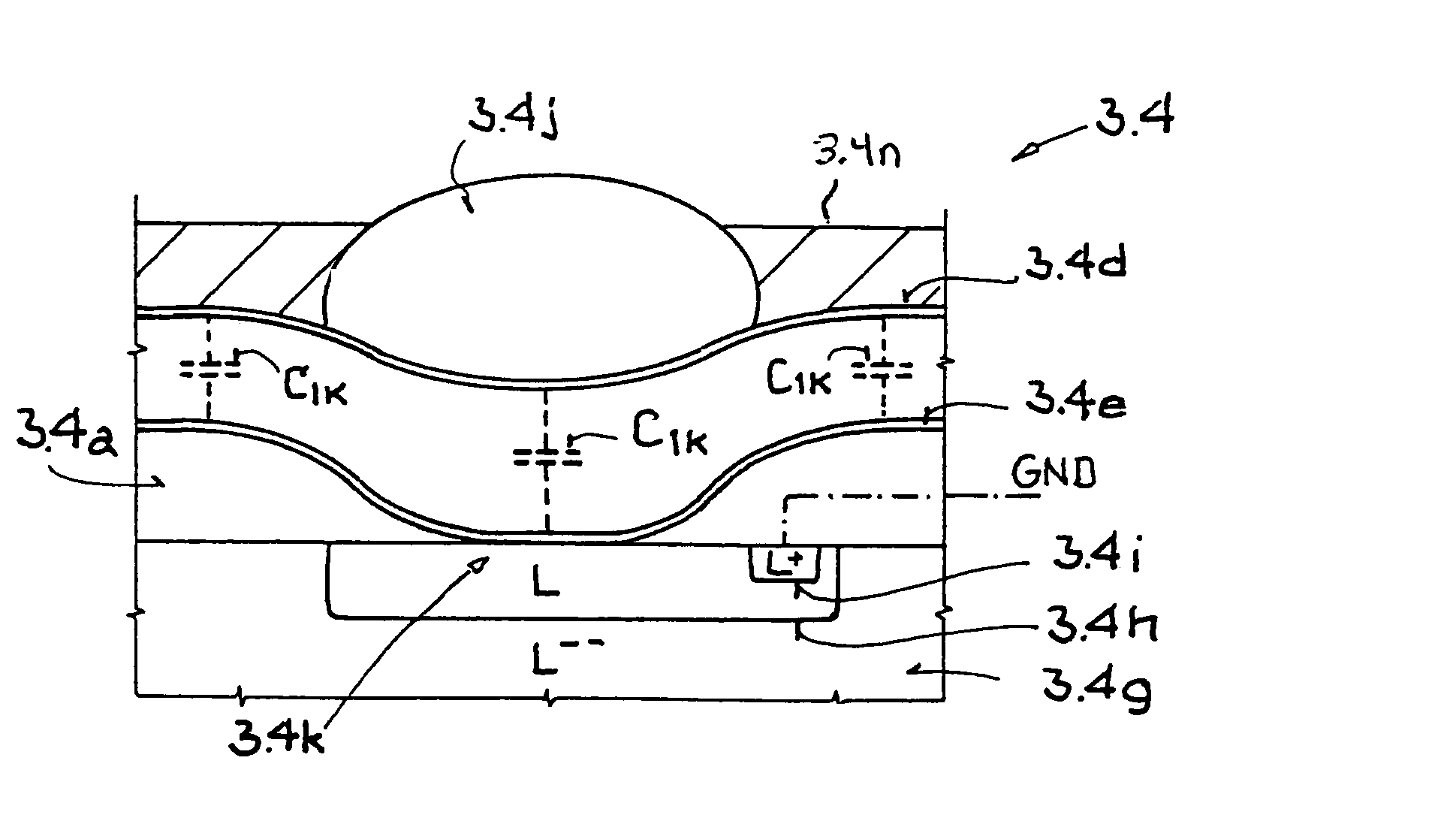
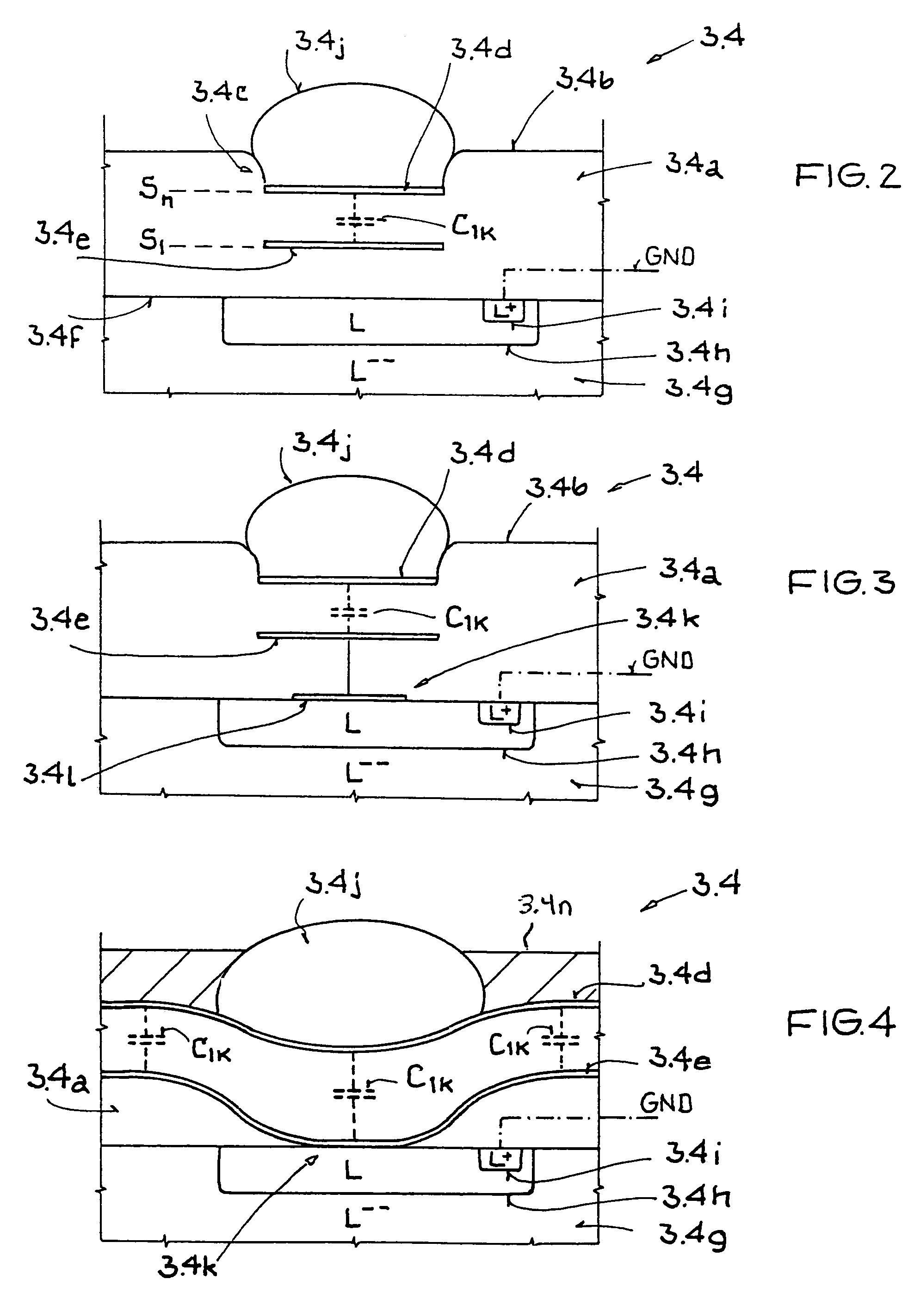
[0029]The transponder 3 has an appropriate receiving device 3.1, for example in the form of a dipole antenna, to receive electrical energy from the HF field 4, the receiving device standing in operative connection with an input pad 3.2 of an integrated circuit 3.3. The input pad 3.2 is part of an inventive semiconductor structure 3.4 which is described in detail below with the aid of FIGS. 2 through 4. In addition, the transponder IC 3.3 from FIG. 1 has a circuit 3.5 within the semiconductor structure 3.4 which can be an RSSI circuit or a rectifier circuit. The former is used to analyze (notch detection) an amplitude-modulated signal (AM signal), and the latter is used to...


PUM


Abstract

A semiconductor structure, for improving rectifier efficiency in passive backscatter transponders or backscatter remote sensors for use in high-frequency electromagnetic fields, is provided. The semiconductor structure has a dielectric layer on whose upper side is arranged a first electrically conductive layer, and a second electrically conductive layer that is spaced apart from the first electrically conductive layer and is arranged essentially below the first electrically conductive layer and is at least partially embedded in the dielectric layer. The dielectric layer has its lower side arranged on a semiconductor substrate of a first conductivity type within which is formed a more highly doped first zone of the first conductivity type which surrounds an even more highly doped second zone of the first conductivity type connected to a reference voltage. Whereby, the first zone can be arranged essentially completely under the first and second electrically conductive layers. In this way, interfering effects of parasitic circuit components can be reduced.

Description

[0001]This nonprovisional application claims priority under 35 U.S.C. §119(a) on German Patent Application No. DE 102004038528, which was filed in Germany on Aug. 7, 2004, and which is herein incorporated by reference.BACKGROUND OF THE INVENTION[0002]1. Field of the Invention[0003]The present invention relates to a semiconductor structure, and further relates to applications of such a semiconductor structure.[0004]2. Description of the Background Art[0005]In RFID or remote sensor systems, use is frequently made today of passive backscatter transponders and remote sensors, which have no internal energy source, for example in the form of a battery, but instead extract the energy needed to power their integrated circuits (IC) from a high-frequency (HF) electromagnetic field radiated from a base station of the system. For this purpose, such transponders or remote sensors contain rectifier circuits which take energy that is transported by an HF carrier wave, captured by a suitable receiv...

Claims


Application Information

Patent Timeline
Patent Type & Authority Patents(United States)
IPC IPC(8): H01L29/94
CPCG06K19/07749H01L23/5223H01L2224/16H01L2924/3011H01L2924/12032H01L2924/01068H01L2924/00H01L24/05H01L24/13H01L2224/05001H01L2224/05027H01L2224/0557H01L2224/05571H01L2224/05572H01L2924/00014H01L2224/05599H01L2224/05099
Inventor FRIEDRICH, ULRICH
Owner ATMEL CORP
Why Eureka
Try Eureka