Bottom anode Schottky diode structure and method

a schottky diode and bottom anode technology, applied in the direction of semiconductor devices, electrical apparatus, transistors, etc., can solve the problems of incompatibility of vertical schottky diodes with cathodes at the bottom of the substrate, limitations on heat dissipation, and inconvenient assembly configuration of vertical schottky diodes, so as to reduce cell pitch and reduce fabrication costs

Inactive Publication Date: 2009-12-15
ALPHA & OMEGA SEMICON LTD
View PDF17 Cites 3 Cited by
  • Summary
  • Abstract
  • Description
  • Claims
  • Application Information

AI Technical Summary

Benefits of technology

[0006]It is therefore an aspect of the present invention to provide a new and improved bottom-anode Schottky (BAS) diode implemented with a combined anode-sinker connected to the bottom of the substrate and a buried Schottky contact. The device configuration has a reduced cell pitch and a planar diode with an N-cathode channel interconnected between the anode-sinker region and a cathode contact. This structure is compatible with many foundries for reducing fabrication costs such that the above discussed technical difficulties and limitations can be overcome.
[0007]Specifically, it is an aspect of the present invention to provide improved bottom-anode Schottky diode device for a boost converter application implemented with a combined anode-sinker connected through a cathode region to a cathode contact along a lateral direction such that a bottom anode connection through the anode sinker significantly reduces the anode inductance, and the use of a substrate source contact minimizes source resistance, and such that the Schottky diodes may be suitable for high gain and high frequency applications.
[0008]It is another aspect of the present invention to provide improved bottom-anode Schottky diode device implemented with a combined anode-sinker connected through a cathode region to a cathode contact along a lateral direction such that the cell pitch can be reduced and the specific on resistance (Rsp) is minimized for a given operating voltage to achieve low forward voltage drop.

Problems solved by technology

Conventional Schottky diodes with a vertical structure that has the cathode disposed at the bottom of a substrate are limited by several difficulties of applications.
As a high voltage bias is applied to the substrate, the vertical Schottky diodes with cathode at the bottom of the substrate are not compatible with some assembly configurations.
Furthermore, for high voltage devices, such device configuration requires an electrical isolation of the heat sink where the die is mounted, which causes limitations on heat dissipation and adds to complications to system designs when the vertical Schottky diodes are provided with the cathode disposed at the bottom of a substrate.
However, the Schottky diodes with a vertical configuration and the cathode on the bottom as shown in these disclosures are still limited by the difficulties discussed above for some practical applications, especially when applied to portable devices that require small package with multi functions to reduce component count and space.
This increases the assembly complexity and cost.

Method used


Image

  • Bottom anode Schottky diode structure and method
  • Bottom anode Schottky diode structure and method
  • Bottom anode Schottky diode structure and method

Examples


Embodiment Construction

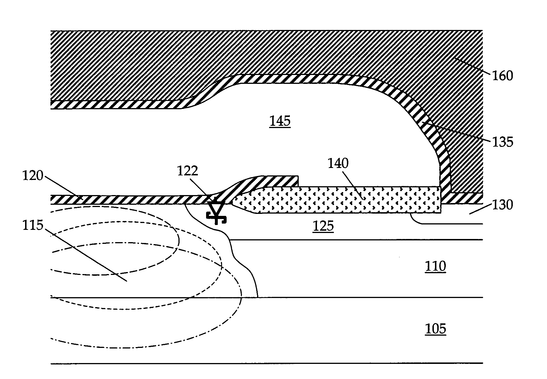
[0023]Referring to FIG. 2 for a cross sectional view of a bottom anode Schottky (BAS) diode device of this invention. The BAS diode device is supported on a P++ substrate 105 functioning as a bottom anode electrode. A layer of P− epitaxial layer 110 is supported on top of the substrate 105. A deep sinker region 115 doped with P+ dopant is disposed below a Schottky barrier metal layer 120, forming an Ohmic contact with Schottky barrier metal 120 and vertically extending to the P++ substrate 105 therefore electrically connecting the substrate bottom metal (not shown) to Schottky barrier metal 120. The Schottky barrier metal 120 extends over a N region 125 forming a Schottky contact (diode) 122 at the interface whereby the N region 125 functions as the Cathode and the Schottky metal layer 120 functions as the Anode of the Schottky diode. An anode to substrate connection is therefore established by the P+ sinker contact electrically with the overlaying Schottky barrier metal 120 and ext...


PUM


Abstract

This invention discloses a bottom-anode Schottky (BAS) diode that includes an anode electrode disposed on a bottom surface of a semiconductor substrate. The bottom-anode Schottky diode further includes a sinker dopant region disposed at a depth in the semiconductor substrate extending substantially to the anode electrode disposed on the bottom surface of the semiconductor and the sinker dopant region covered by a buried Schottky barrier metal functioning as an Schottky anode. The BAS diode further includes a lateral cathode region extended laterally from a cathode electrode near a top surface of the semiconductor substrate opposite the Schottky barrier metal wherein the lateral cathode region doped with an opposite dopant from the sinker dopant region and interfacing the sinker dopant region whereby a current path is formed from the cathode electrode to the anode electrode through the lateral cathode region and the sinker dopant region in applying a forward bias voltage and the sinker dopant region depleting the cathode region in applying a reverse bias voltage for blocking a leakage current.

Description

BACKGROUND OF THE INVENTION[0001]1. Field of the Invention[0002]The invention relates generally to the Schottky diode devices. More particularly, this invention relates to a device configuration and method of manufacturing Schottky diodes with a bottom-anode for multiple applications.[0003]2. Description of the Prior Art[0004]Conventional Schottky diodes with a vertical structure that has the cathode disposed at the bottom of a substrate are limited by several difficulties of applications. As a high voltage bias is applied to the substrate, the vertical Schottky diodes with cathode at the bottom of the substrate are not compatible with some assembly configurations. Furthermore, for high voltage devices, such device configuration requires an electrical isolation of the heat sink where the die is mounted, which causes limitations on heat dissipation and adds to complications to system designs when the vertical Schottky diodes are provided with the cathode disposed at the bottom of a s...

Claims


Application Information

Patent Timeline
Patent Type & Authority Patents(United States)
IPC IPC(8): H01L27/095H01L29/04H01L29/47H01L29/49H01L29/74H01L29/80H01L29/812H01L31/00H01L31/07H01L31/108H01L31/111H01L31/112
CPCH01L29/402H01L29/66143H01L29/861H01L29/872H01L2924/0002H01L2924/00
Inventor HEBERT, FRANCOIS
Owner ALPHA & OMEGA SEMICON LTD
Why Eureka
Try Eureka