Sheet-like electronic component clean transfer device and sheet-like electronic component manufacturing system

a technology of electronic components and manufacturing systems, applied in the field of sheet-like electronic components clean transfer devices and sheet-like electronic component manufacturing systems, can solve the problems of increasing the cost of facility installation of expensive computer-controlled systems, and achieve the effects of reducing the fluctuation of air pressure, stable cleanliness, and large internal pressure differences

Inactive Publication Date: 2009-12-22
RORZE CORP
View PDF23 Cites 19 Cited by
  • Summary
  • Abstract
  • Description
  • Claims
  • Application Information

AI Technical Summary

Benefits of technology

[0004]As a result of dedicated examinations for solving the above-described problems, the present inventor has found out that a very high clean state of the class 1 can be maintained with respect to particles of 0.1 μm even in the operation by using a filter which removes 99.999% or more of particles of 0.1 μm or above in a fan / filter unit, horizontally providing a floor (which will be referred to as a “first floor” hereinafter) which is positioned below an arm at a middle height part of a conveying robot and through which air flows, partitioning a first chamber between the fan / filter unit and the first floor and partitioning a second chamber between a bottom part of the casing through which air can flow to the outside and the first floor by the casing in an apparatus which automatically transfers by a conveying robot in the casing a sheet-like electronic component between predetermined positions, e.g., a cassette, a hard lock chamber such as a processing chamber and the like in clean air which has passed through the fan / filter unit provided on the ceiling of the casing.
[0006]The present inventor has found out that a further advantage can be obtained by horizontally arranging a second floor which is positioned in the vicinity of a base of the conveying robot and through which air passes as well as the first floor and changing a degree of opening of the bottom part of the casing with respect to the outside, and thereby developed the transfer device in which a space where a sheet-like electronic component such as a wafer is transferred is very cleaned.
[0009]This gap can suppress a fluctuation in air pressure in a space where a sheet-like electronic component exists to the minimum level, and prevent foreign particles from being suspended with a minimum disturbance of an air current. When the gap is not provided, an exhaust air stream depends on only a degree of opening of the first floor through which air passes. Therefore, an internal pressure of the first chamber reaches up to 25 Pa, and it is reduced to 1 / 1.3 to ½ all at once when the door is opened. Not only a disturbance in an air current is generated due to sudden exhaust around the door, but also an eddy current may be generated in some cases due to a disturbance in the air current even around an arm of the conveying robot or a wafer in the chamber, and there occurs an inconvenience that foreign particles are involved in this eddy current or foreign particles in the eddy current cannot be discharged, for example. If the gap is as narrow as 1 mm or below, such a large internal pressure difference as described above cannot be eliminated. On the contrary, if the gap is too large, foreign particles are apt to be diffused or enter from the outside. The present inventor has discovered from an experiment and an experience that a limit of the gap is 30 mm on the maximum level.
[0010]Additionally, when an air pressure in the first chamber on the upper side of the first floor in the casing is set higher than that of the second chamber on the lower side of the first floor in the casing and air pressures in the both chambers are set to be higher than that of the outside of the casing, a stable cleanliness can be maintained in the first chamber. Here, it is preferable for the second chamber to maintain at least 0.1 Pa from the outside of the casing.
[0013]Next, in the transfer device according to the present invention, it is preferable to move up and down the door and cover a door passage provided on the second chamber side on the lower side of the first floor with a partition in order to realize movement of the door. Then, clean air which flows into the second chamber from the first chamber is directly discharged to the outside of the casing through the passage, thereby preventing the door from being contaminated. Furthermore, as to the door, a lid on the front part of a cassette for a wafer such as an FOUP (Front Opening Unified Pod) may be sucked and fixed to the door, and it may be moved up and down together with the door.
[0016]Additionally, the present invention also provides a sheet-like electronic component manufacturing facility which utilizes the above-described transfer device which prevents infiltration of foreign particles and contamination due to organic matters. In this facility, a cassette station for a cassette which accommodates and conveys a sheet-like electronic component is coupled with a processing chamber in which various kinds of processing such as resist coating, pre-baking, exposure, development, post-baking, etching, cleansing and others are performed with the transfer device being interposed.

Problems solved by technology

Further, in the apparatus disclosed in Japanese Patent Application Laid-open No. 2001-244315, there is a case in which a robot or an opening / closing door as a foreign particle generation source moves in a clean booth or a case in which foreign particles soar above with eddy currents generated on the rear side of a sheet-like matter, a cleanness is insufficient, and installation of an expensive computer-controlled system increases a facility cost, which is not desirable.

Method used


Image

  • Sheet-like electronic component clean transfer device and sheet-like electronic component manufacturing system
  • Sheet-like electronic component clean transfer device and sheet-like electronic component manufacturing system
  • Sheet-like electronic component clean transfer device and sheet-like electronic component manufacturing system

Examples


embodiment 1

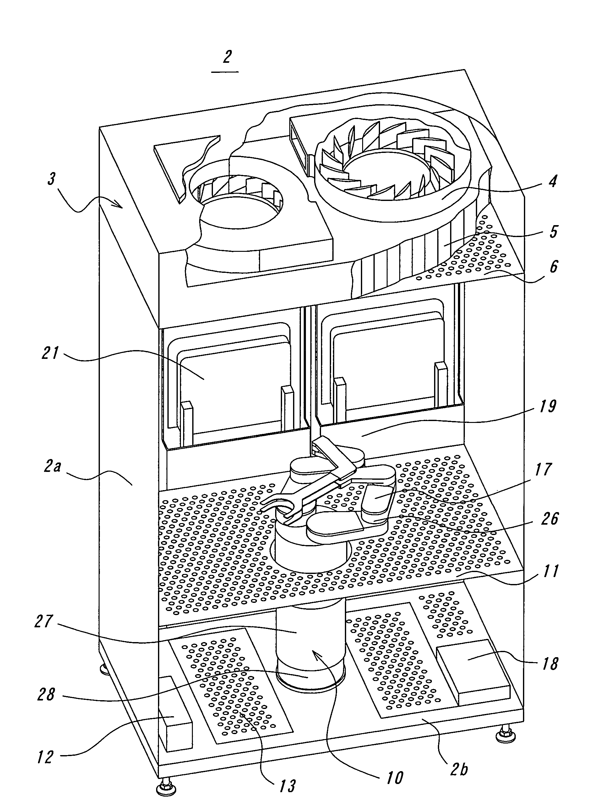
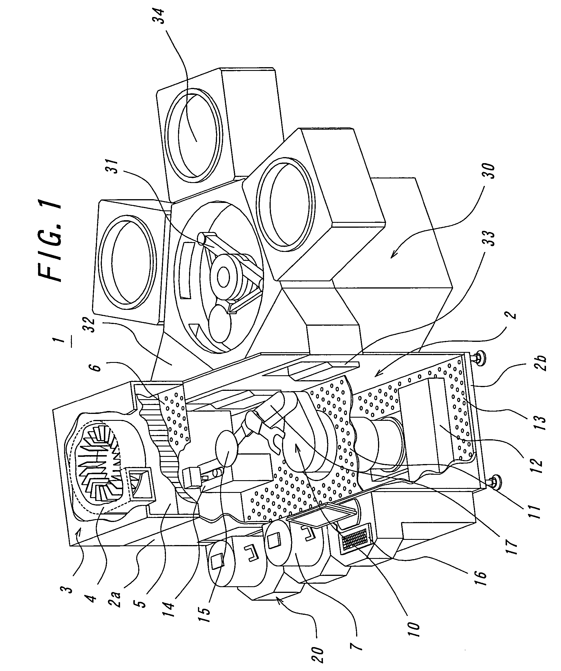
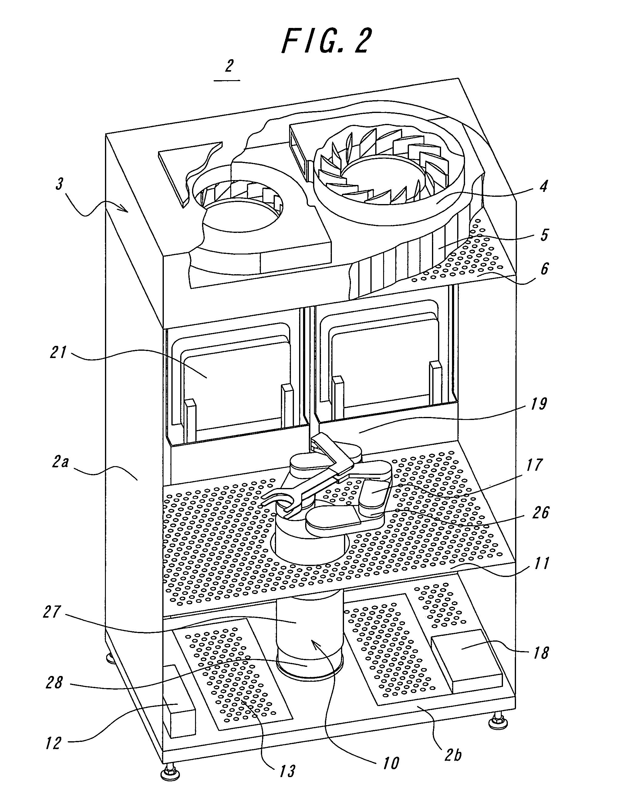
[0035]A punching plate (a perforated plate) in which a hole of 4 mm φ is opened at each apex of a regular triangle having each side of 8 mm was used, and its degree of opening was 20% when all opening parts, i.e., the gap having a width of 5 mm at the body rim of the conveying robot 10, the gap having a width of 6 mm around the door 21 and the elevating passage part of the door 21 were added up. The conveying robot 10, the power supply device 18, the control device 12 and others were set on the bottom part frame 2b, but the second floor 13 formed of a punching plate was not set in particular, and the degree of opening of the bottom part frame 2b reached 53%.

[0036]Clean air was sampled immediately above the wafer and immediately below the wafer stopped in a state where the wafer is mounted on the fingers of the conveying robot 10 while changing a blowing speed from the fan / filter unit 3 from 0.05 m / second to 0.65 m / second and changing a position of the wafer between the two FOUPs by ...

embodiment 2

[0039]This embodiment has the same structure as Embodiment 1 except that the degree of opening of the bottom part frame 2b is set to 25% by laying a punching plate as the second floor 13 at a part of the bottom part frame 2b, and results are all shown in Table 1. There is no problem except that 0.3 foreign particles are observed immediately below the wafer at a wind speed of 0.65 m / second. Although ventilation is not sufficient when the number of times of ventilation is 4.8 or below / minute, the class 1 is maintained with the number of times of ventilation up to 41.5 / minute, and it was found that the effect of the second floor is demonstrated.

embodiment 3

[0040]This embodiment has the same structure as Embodiment 2 except that the degree of opening of the first floor is reduced to 5%, and results are all shown in Table 1. There is no problem except that 0.3 foreign particle is observed immediately below the wafer at a wind speed of 0.6 m / second and 2.3 foreign particles are observed immediately below the wafer at a wind speed of 0.65 m / second (the number of times of ventilation is 41.5). That is, the class 1 is satisfied in a range of 0.1 m / second to 0.6 m / second.


PUM


Abstract

When a first floor (11) which is formed of a punching plate or the like and through which air passes is provided immediately below an arm (17) at a middle height part of a conveying robot (10) in a casing (2a) of a clean transfer device (2) and a degree of opening of a casing bottom part frame (2b), which supports a base part of the conveying robot (10), with respect to the outside is restricted, a class 1 can be maintained. Here, when a second floor (13) formed of a punching plate or the like is used on the casing bottom part frame (2b), a class 0 state can be realized under specific conditions, thereby enabling production of a semiconductor having a wire width of 0.1 μm. As a result, the device can cope with the unexpectedly high degree of cleanliness of 0.1 μm particle class 1, which cannot be realized in the prior art, requested also for the transfer device according to a reduction in wire width on a highly integrated semiconductor wafer.

Description

TECHNICAL FIELD[0001]The present invention relates to a transfer device including a clean booth, which transfers a product such as a semiconductor wafer, a liquid crystal display unit, a plasma display unit, organic and inorganic electroluminescences, a field emitting display unit, a printed wiring board and others and a sheet-like electronic component used in such a product between a cassette as a cleaning vessel and various kinds of processing devices under a clean environment, and to a sheet-like electronic component manufacturing facility which uses this transfer device.BACKGROUND ART[0002]In a conventional clean booth as a cleaning space, as disclosed in, e.g., Japanese Patent Application Laid-open No. 1990-4145, there has been adopted a method by which clean air supplied from an HEPA (High Efficiency Particulate Air) filter or a ULPA (Ultra Low Penetration Air) filter set on a ceiling of a box-like body blows down foreign particles and these foreign particles are discharged to...

Claims


Application Information

Patent Timeline
Patent Type & Authority Patents(United States)
IPC IPC(8): H01L21/677B65G49/00F24F7/06H01L21/00H01L21/02H01L21/50
CPCH01L21/67017F24F7/06H01L21/02H01L21/68
Inventor SAKIYA, FUMIO
Owner RORZE CORP
Why Eureka
Try Eureka