
Method for manufacturing a laterally diffused metal oxide semiconductor device

a metal oxide semiconductor and laterally diffused technology, applied in the field of semiconductor devices, can solve the problems of device failure, uncontrollable diffusion of boron implants, and undesirable regions of boron implanted atoms, and achieve the effect of reducing the number of silicon defects, being reliable and cost-effectiv

Active Publication Date: 2009-12-29
BELL SEMICON LLC +1
View PDF2 Cites 97 Cited by
  • Summary
  • Abstract
  • Description
  • Claims
  • Application Information

AI Technical Summary

Benefits of technology

"The present invention provides a method for manufacturing a laterally diffused metal oxide semiconductor (LDMOS) device that does not experience uncontrollable boron diffusion and reduces the number of silicon defects resulting from the prior art boron implants. This method involves forming an amorphous region in a semiconductor substrate and diffusing a channel dopant from the amorphous region to form a first portion of a channel. The inclusion of the amorphizing element within the semiconductor substrate makes the manufacturing process more reliable and cost efficient."

Problems solved by technology

One drawback currently experienced during manufacturing LDMOS devices is an uncontrollable diffusion of the boron implant, resulting from variations in a desired implanted profile.
Typically, the problem is a result of the fairly high kinetic energy imparted on the boron implanted atoms, and collisions that occur between such atoms in a lattice of the substrate material.
These collisions tend to cause a portion of the boron implanted atoms to locate in an undesirable region of the device in a process called channeling.
The uncontrollable diffusion, if extreme enough, may also cause device failure.

Method used


Image

  • Method for manufacturing a laterally diffused metal oxide semiconductor device
  • Method for manufacturing a laterally diffused metal oxide semiconductor device
  • Method for manufacturing a laterally diffused metal oxide semiconductor device

Examples


Embodiment Construction

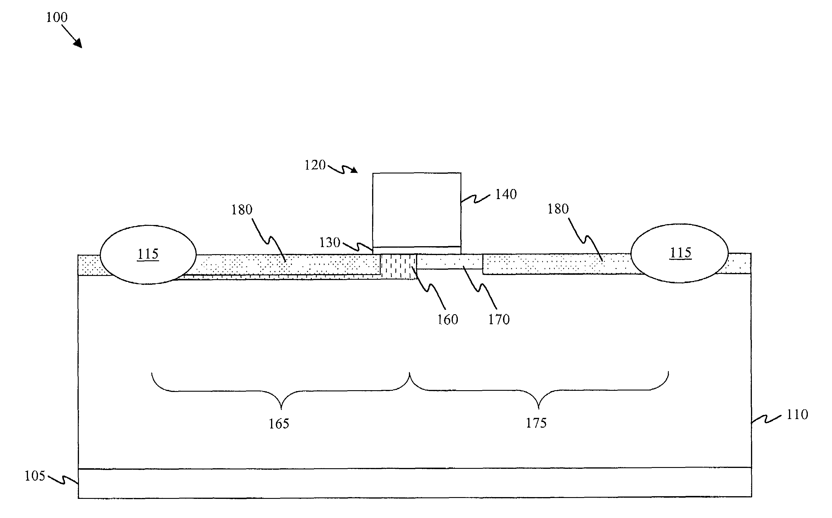
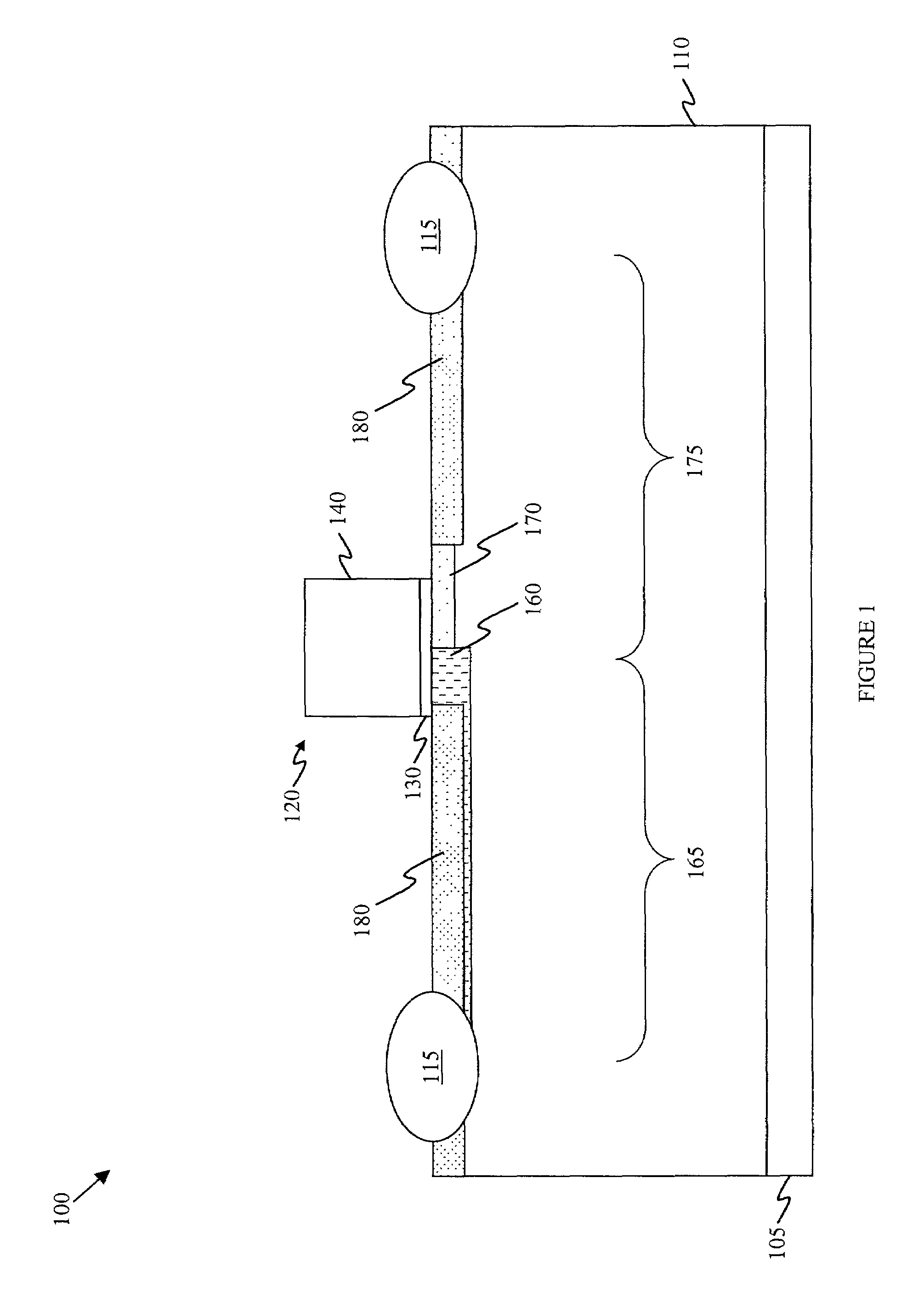
[0020]Referring initially to FIG. 1, illustrated is a cross-sectional view of a completed laterally diffused metal oxide semiconductor (LDMOS) device 100 manufactured by the method described herein. The LDMOS device 100 includes a semiconductor wafer 105, a semiconductor substrate 110, and first and second isolation structures 115. It should be noted that the semiconductor substrate 110 may be any layer located in the LDMOS device 100, including the semiconductor wafer 105 or a layer located above the semiconductor wafer 105.

[0021]The LDMOS device 100 further includes a gate structure 120 located over the semiconductor substrate 110 and between the first and second isolation structures 115. The gate structure 120, in the illustrative embodiment, includes a conventional gate oxide 130 and poly gate 140. As illustrated, a channel dopant 160 is located on a side of the gate structure 165. Because of the unique method of manufacturing the LDMOS device 100, which will be discussed in gre...


PUM

PropertyMeasurementUnit
depthaaaaaaaaaa
depthaaaaaaaaaa
temperatureaaaaaaaaaa

Abstract

A laterally diffused metal oxide semiconductor (LDMOS) device and a method of manufacture therefor. The method of manufacturing the LDMOS device includes forming an amorphous region in a semiconductor substrate between isolation structures and adjacent a gate structure, by implanting an amorphizing element, such as silicon or germanium, in the semiconductor substrate. The method further includes diffusing a channel dopant laterally in the amorphous region, to form a first portion of a channel.

Description

CROSS-REFERENCE TO PROVISIONAL APPLICATION[0001]This application claims the benefit of U.S. Provisional Application No. 60 / 174,549, entitled “INTEGRATED CIRCUIT AND A METHOD OF MAKING AN INTEGRATED CIRCUIT,” to Charles Walter Pearce, filed on Jan. 5, 2000, which is commonly assigned with the present invention and incorporated herein by reference as if reproduced herein in its entirety.TECHNICAL FIELD OF THE INVENTION[0002]The present invention is directed, in general, to a semiconductor device and, more specifically, to a laterally diffused metal oxide semiconductor (LDMOS) device and a method of manufacture therefor.BACKGROUND OF THE INVENTION[0003]Power semiconductor devices are currently being used in many applications, either as discrete components or integrated with other transistors as an integrated circuit. Such power devices include high-voltage integrated circuits which typically include one or more high-voltage transistors, often on the same chip as low-voltage circuitry. ...

Claims


Application Information

Patent Timeline
Patent Type & Authority Patents(United States)
IPC IPC(8): H01L21/336H01L21/265
CPCH01L29/66659H01L21/26506
Inventor PEARCE, CHARLES W.
Owner BELL SEMICON LLC
Learn More