Semiconductor device and method of manufacturing the same

a semiconductor device and semiconductor technology, applied in the field of semiconductor devices, can solve problems such as the downsizing of semiconductor devices, and achieve the effect of effectively solving problems

Active Publication Date: 2010-01-05
SHINKO ELECTRIC IND CO LTD
View PDF5 Cites 7 Cited by
  • Summary
  • Abstract
  • Description
  • Claims
  • Application Information

AI Technical Summary

Benefits of technology

[0009]The present invention has been achieved in view of the above, and an object of the present invention is to provide, in particular, small semiconductor device and a manufacturing method thereof and also effectively solve problems such as variations in strength of a bonding part, occurring in the fabrication process.
[0021]According to the first aspect of the present invention, one pad for serving as a fiducial mark (hereinafter called fiducial mark pad) has effects of functioning as a pad and also functioning as a fiducial mark. Therefore, it becomes unnecessary to separately provide a region for forming a dedicated fiducial mark in the inner periphery or the outer periphery of a pad region as shown in the conventional semiconductor device, so that a substrate and a lower package can be downsized.
[0022]According to the second aspect of the present invention, a fiducial mark pad is formed in a shape different from other pads, so that a position of the fiducial mark pad can be recognized while distinguishing the fiducial mark pad from the other pads by a recognition device. Further, the fiducial mark pad and the other pads are formed such that an area of the fiducial mark pad is substantially equal to an area of the other pads, so that the areas, where solder in the fiducial mark pad and the other pads wetly spreads in bonding an upper package to a lower package, can be substantially equalized, and bonding strength and a formation shape of the solder is not adversely affected and a uniform bonding without variations can be achieved.
[0023]According to the third and fourth aspects of the present invention, accuracy of position recognition of a lower package can be improved by a configuration in which fiducial mark pads are provided in plural places, for example, in two places in diagonal positions or in three places in positions forming a triangle.
[0024]According to the fifth aspect of the present invention, a step for forming a dedicated fiducial mark can be omitted, and a work period and material cost necessary for the formation can be reduced. Also, a substrate and a lower package can be formed smaller than those of the conventional art and the number of packages capable of being placed in a carrier can be increased, so that production efficiency of a semiconductor device can be improved.

Problems solved by technology

However, in the PoP technique for downsizing the semiconductor device, for example, like the conventional semiconductor device shown in FIG. 7, the configuration where the recognition bump etc. for recognizing a package position in a manufacturing process hinders downsizing of the semiconductor device.

Method used


Image

  • Semiconductor device and method of manufacturing the same
  • Semiconductor device and method of manufacturing the same
  • Semiconductor device and method of manufacturing the same

Examples


Embodiment Construction

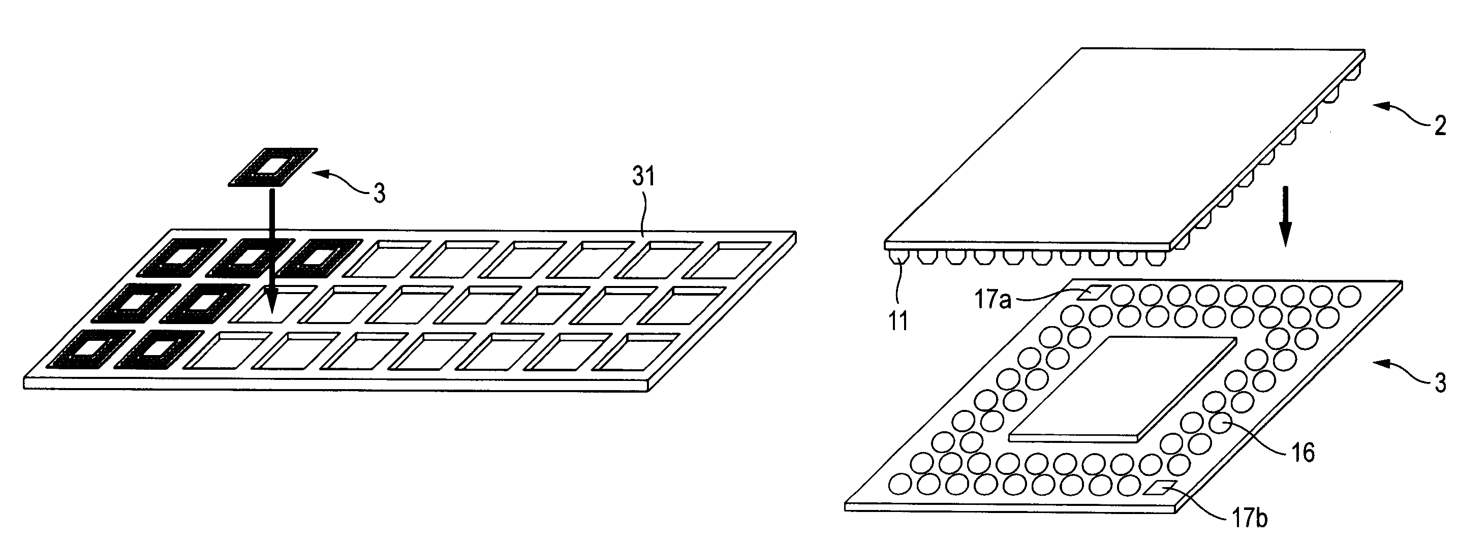
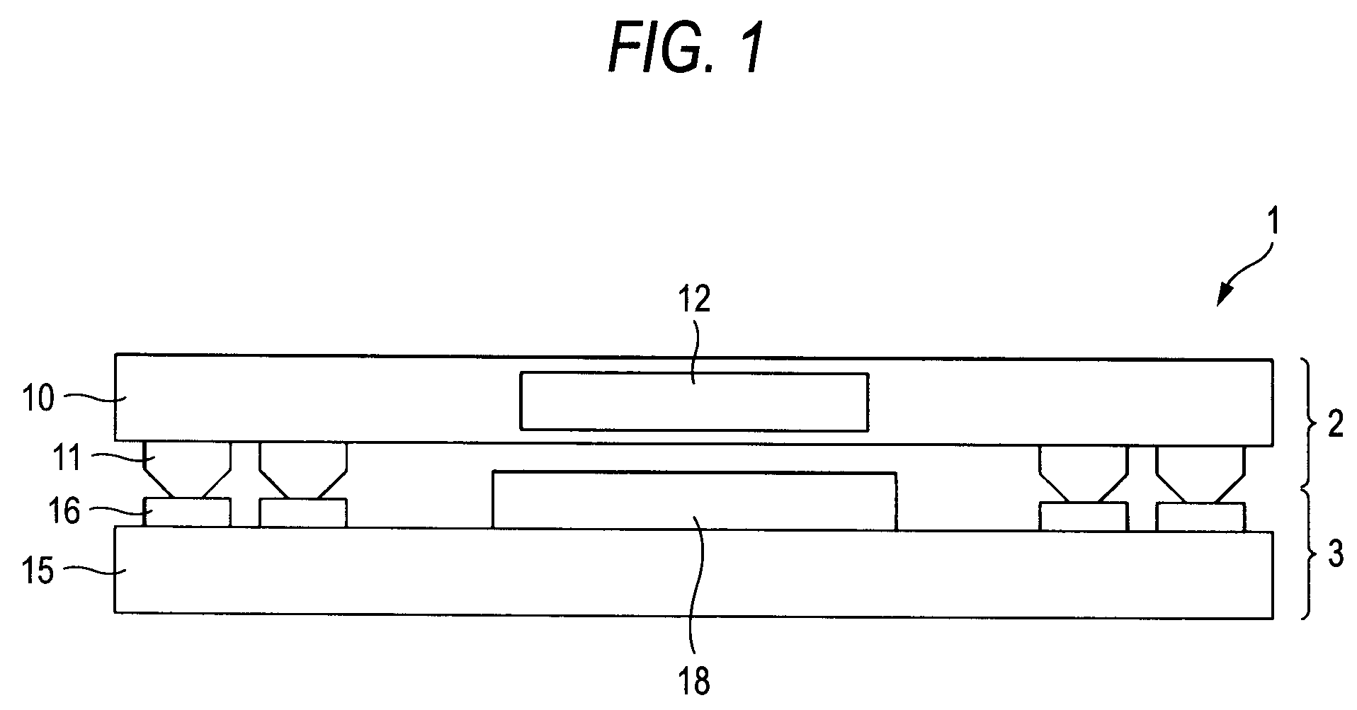
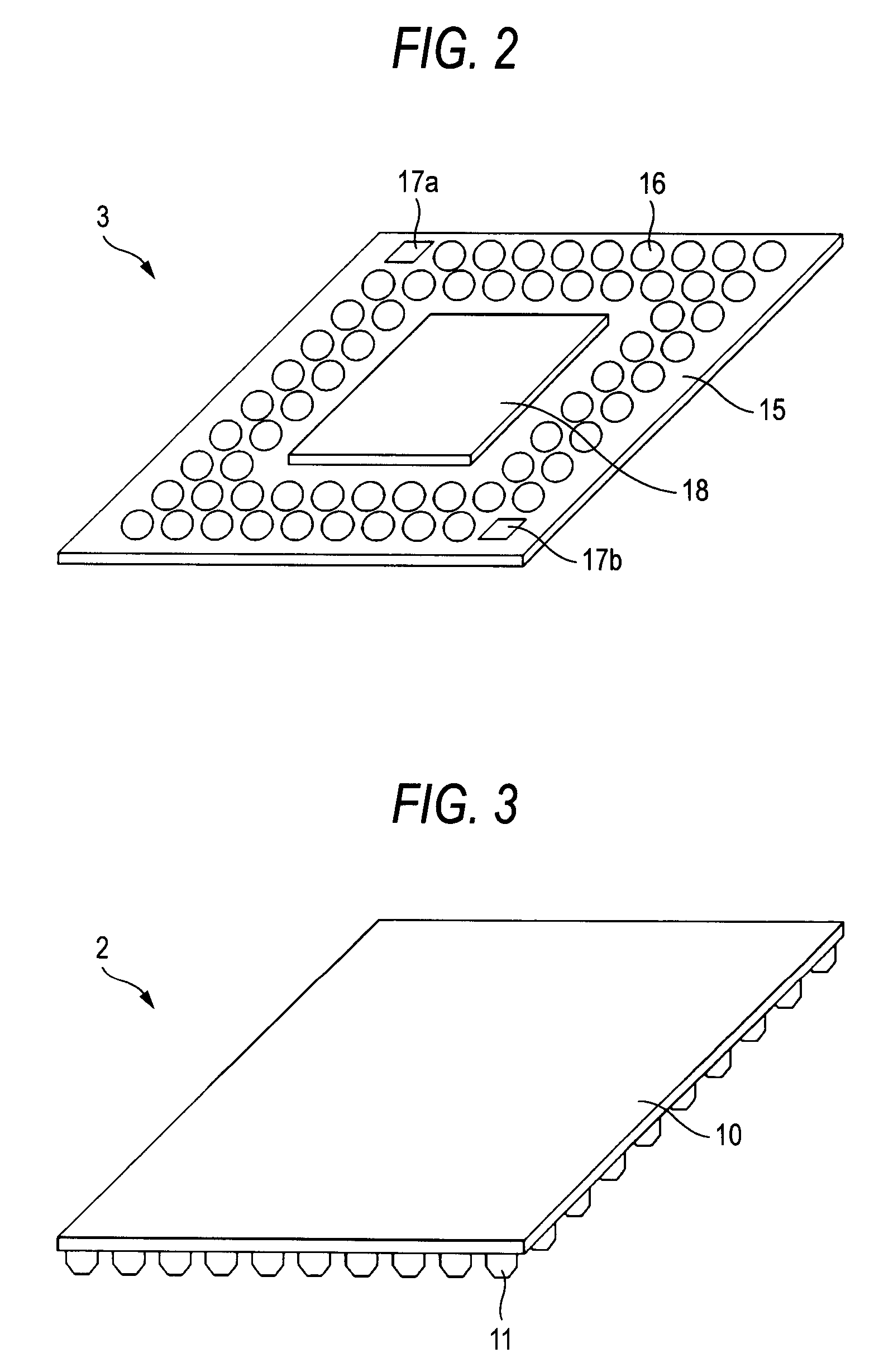
[0032]Embodiments of the invention will hereinafter be described in detail with reference to the drawings. FIG. 1 is a sectional view showing one example of a semiconductor device 1 according to an embodiment of the invention. Also, FIG. 2 is a schematic view showing a configuration of a lower package 3 of the semiconductor device 1. FIG. 3 is a schematic view showing a configuration of an upper package 2 of the semiconductor device 1. FIGS. 4A to 4C are schematic views describing a manufacturing method of the semiconductor device according to the embodiment of the invention. FIG. 5 is a schematic view showing a configuration of a lower package 3 of a semiconductor device 1 according to a second embodiment of the invention. In addition, in numerals of the drawings, numeral 17 is used as a generic term of numerals 17a to 17e.

[0033]The semiconductor device 1 as shown in FIG. 1 is configured by directly connecting solder balls 11 of an upper package 2 to pads 16 (and fiducial mark pad...


PUM


Abstract

A semiconductor device includes: solder balls provided on an upper package; and pads provided on a lower package and directly connected to the solder balls, wherein at least one of the pads serves as a fiducial mark. Further, a shape of at least one of the pads is different from that of other pads and an area of at least one of the pads is substantially equal to that of the other pads.

Description

[0001]This application is based on and claims priority from Japanese Patent Application No. 2006-333998, filed on Dec. 12, 2006, the entire contents of which are hereby incorporated by reference.BACKGROUND OF THE INVENTION[0002]1. Technical Field[0003]The present disclosure relates to a semiconductor device and a method of manufacturing the same, and more particularly to a semiconductor device formed by directly connecting a solder ball of an upper package to a pad of a lower package and a manufacturing method thereof.[0004]2. Background Art[0005]There is a Package on Package (PoP) technique as one of the important element techniques for downsizing, thinning, etc. in electronic equipment. As a typical example of the PoP technique, a configuration of directly connecting a solder ball of an upper package to a pad of a lower package is given, and a semiconductor device with high density and high performance can be achieved.[0006]In the PoP technique, accuracy of recognition of a packag...

Claims


Application Information

Patent Timeline
Patent Type & Authority Patents(United States)
IPC IPC(8): H01L23/544
CPCH01L23/544H05K1/0269H05K3/303Y02P70/613H01L2223/54426H01L2223/54473H01L2223/54486H01L2224/16H01L2924/15311H05K1/111H05K2201/09381H05K2201/094H05K2201/10734H05K2203/166H01L2221/68313Y02P70/50H01L23/48
Inventor KASUGA, TAKAHIRO
Owner SHINKO ELECTRIC IND CO LTD
Why Eureka
Try Eureka